X-ray inspection device and X-ray inspection method

a technology of x-ray inspection and inspection method, which is applied in the direction of feeding apparatus, electron beam welding apparatus, using electrical/magnetic means, etc., can solve the problems of failure to inspect the failure of the solder ball to be partially bonded to the land, and the hardly formed side of the solder bump

Active Publication Date: 2009-12-29
DENSO CORP
View PDF9 Cites 5 Cited by
  • Summary
  • Abstract
  • Description
  • Claims
  • Application Information

AI Technical Summary

Benefits of technology

[0010]When the circuit device having a solder ball is mounted on the printed circuit board including a land disposed separately from the resist, the solder ball is melted so that the solder ball is normally bonded to the land. In this state, the solder bump is formed on the top and on the side of the land. However, when the solder ball and the land are not completely bonded together so that the solder ball is separated from the land or the solder ball is partially bonded to the land, the solder bump is hardly formed on the side of the land. Accordingly, the X-ray is irradiated to the solder connection portion in a state where the circuit device is mounted on the printed circuit board, and the horizontal tomographic image showing existence or nonexistence of the solder bump is formed and outputted on the basis of the X-ray transmitted through the solder connection portion. Thus, not only the floating failure of the solder ball but also the failure that the solder ball is partially bonded to the land can be inspected. Therefore, the failure of the solder connection portion is reliably inspected.

Problems solved by technology

However, when the solder ball and the land are not completely bonded together so that the solder ball is separated from the land or the solder ball is partially bonded to the land, the solder bump is hardly formed on the side of the land.
Thus, not only the floating failure of the solder ball but also the failure that the solder ball is partially bonded to the land can be inspected.

Method used


Image

  • X-ray inspection device and X-ray inspection method
  • X-ray inspection device and X-ray inspection method
  • X-ray inspection device and X-ray inspection method

Examples


first embodiment

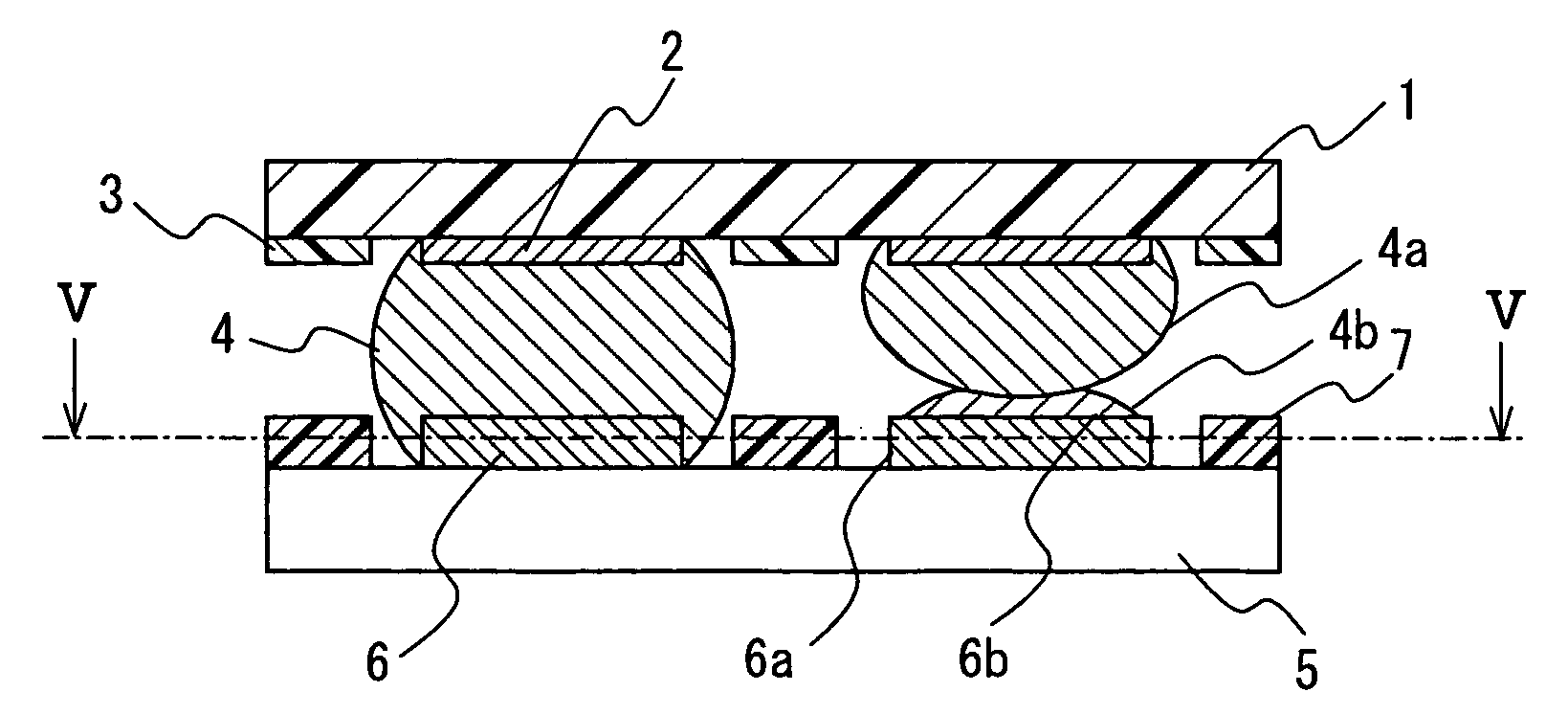
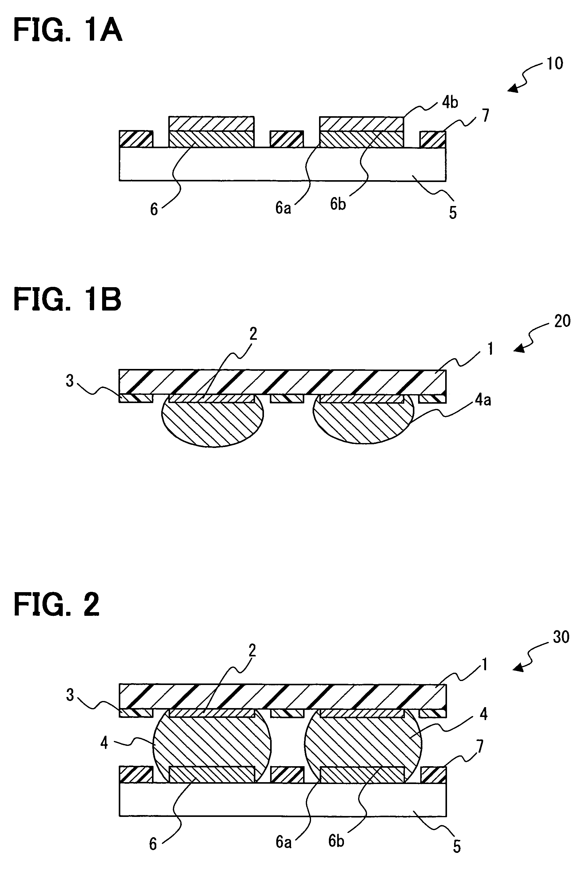
[0024]A first embodiment of the present invention is explained with reference to drawings as follows. FIG. 1A is a partial cross sectional view showing a schematic constitution of a printed circuit board according to the first embodiment of the present invention. FIG. 1B is a partial cross sectional view showing a schematic constitution of a circuit device according to the first embodiment of the present invention. FIG. 2 is a partial cross sectional view showing a schematic constitution of a state where the circuit device is mounted on the printed circuit board according to the first embodiment of the present invention.

[0025]Firstly, an electric device 30 as an object of inspection according to the embodiment of the present invention is explained. The electric device 30 includes a printed circuit board 10 and a circuit device 20.

[0026]As shown in FIG. 1A, the printed circuit board 10 according to the embodiment of the present invention includes a printed circuit board side solder 4...

second embodiment

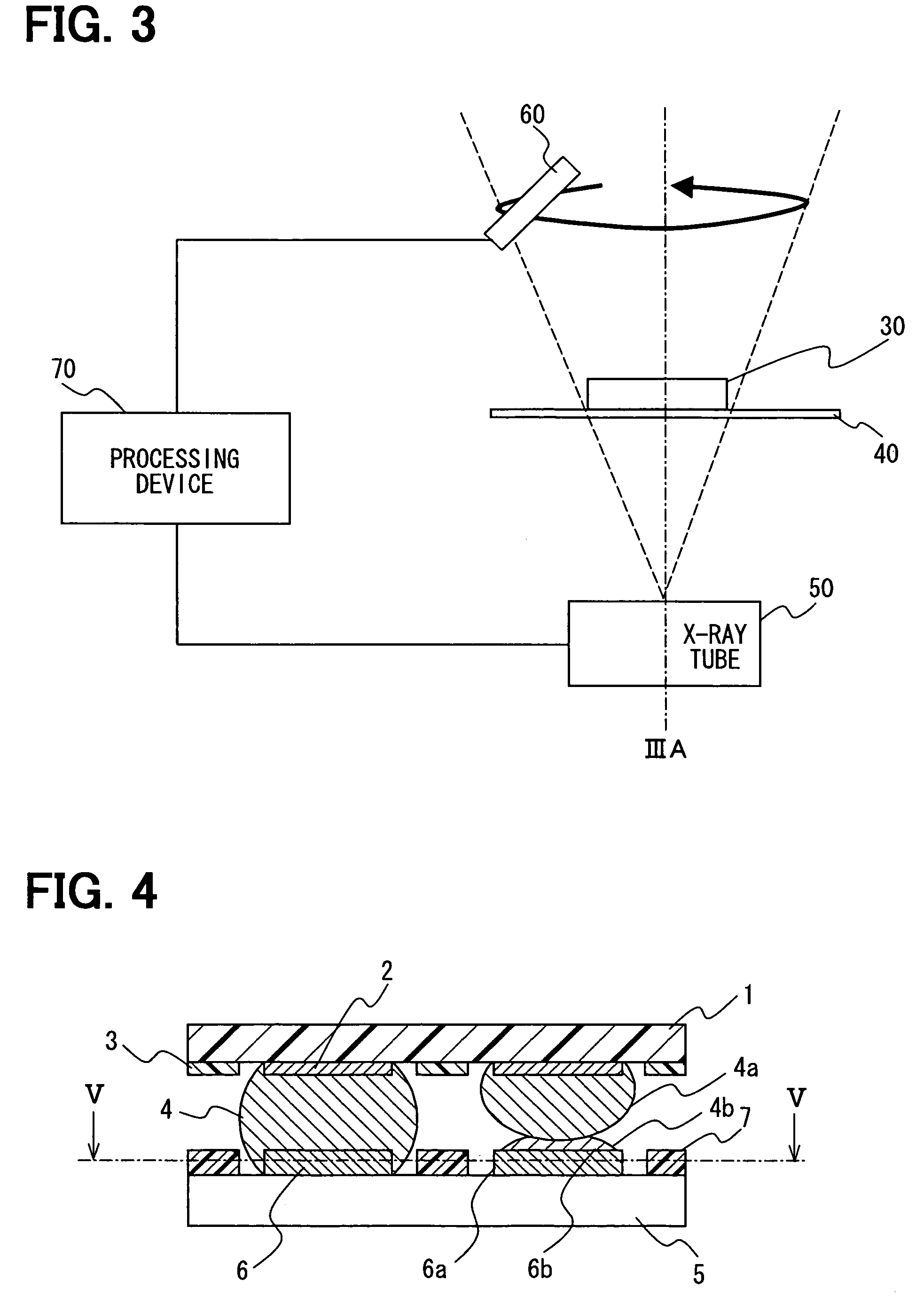
[0064]Next, second embodiment of the present invention is explained with reference to the drawings. FIG. 7A is a partial cross sectional view showing a schematic constitution of a state that the circuit device is mounted on the printed circuit board according to the second embodiment of the present invention. FIG. 7B is a partial plan view showing a schematic constitution of the printed circuit board according to the second embodiment of the present invention. FIG. 8 is a partial cross sectional view showing a case where the warpage compensation marks of the circuit device and the printed circuit board are arranged at different points, according to the second embodiment of the present invention. FIG. 9 is an explanation view showing a schematic constitution of a warpage measurement device according to the second embodiment of the present invention.

[0065]Here, the X-ray inspection device according to the second embodiment inspects the connection state of the solder connection portion...


PUM

PropertyMeasurementUnit
thicknessaaaaaaaaaa
distanceaaaaaaaaaa
distanceaaaaaaaaaa

Abstract

A X-ray inspection device for inspecting a solder connection portion between a circuit device having a solder ball and a printed circuit board having a land includes: X-ray irradiating means for irradiating X-ray to the solder connection portion between the solder ball and the land; X-ray detecting means for detecting the X-ray transmitted through the solder connection portion and for outputting a detection signal; and image forming means for forming and outputting a horizontal tomographic image of the solder connection portion on the basis of the detection signal. The horizontal tomographic image shows existence or nonexistence of a solder bump disposed on a side of the land.

Description

CROSS REFERENCE TO RELATED APPLICATIONS[0001]This application is based on Japanese Patent Applications No. 2005-56640 filed on Mar. 1, 2005, and No. 2005-349606 filed on Dec. 2, 2005, the disclosures of which are incorporated herein by reference.FIELD OF THE INVENTION[0002]The present invention relates to a X-ray inspection device and a X-ray inspection method.BACKGROUND OF THE INVENTION[0003]Conventionally, a X-ray inspection method for inspecting a connection state of a solder connection portion between a circuit device and a printed circuit board is disclosed in U.S. Pat. No. 6,823,040. A solder ball is formed in a lattice pattern on one side of the circuit device, and a land is formed on a position of the printed circuit board corresponding to the solder ball.[0004]The X-ray inspection method disclosed in U.S. Pat. No. 6,823,040 includes a step of mounting a sample on a table, the sample in which the circuit device is mounted on the printed circuit board. Then, a X-ray source is...

Claims


Application Information

Patent Timeline
Patent Type & Authority Patents(United States)
IPC IPC(8): B23K31/12
CPCB23K31/12H05K3/3436H05K1/0269G01R31/309
Inventor HIRAMATSU, TOMOYUKIHAYASHI, YOSHINORIHASEGAWA, HISASHI
Owner DENSO CORP
Why Eureka
Try Eureka