Test chip socket and method for testing a chip

a chip and socket technology, applied in the field of test chip sockets, can solve the problems of increasing the test cost, the inability to insert the test target chip into the test chip socket, and the limited size of the tester substrate, so as to achieve the effect of further reducing the cost of testing the chipped circui

Inactive Publication Date: 2010-01-05
YAMAHA CORP
View PDF16 Cites 2 Cited by
  • Summary
  • Abstract
  • Description
  • Claims
  • Application Information

AI Technical Summary

Benefits of technology

[0008]It is an object of the present invention to provide a test chip socket to reduce a cost of testing a chipped circuit.
[0010]According to the above-described test chip socket, in a condition that the tray is removed from the contact block, a plurality of test target chips can be mounted to the plurality of mount positions of one tray and removed from tray; therefore, a process for mounting or removing a test target chip can be automated by using a handler. Moreover, a plurality of test target chips can be fixed to one contact block; therefore, the test target chips can be tested in a condition that the chips are arranged densely to the tester substrate. Therefore, this test chip socket can reduce a cost for testing a chipped circuit.
[0015]According to this test system, a cost for testing signal processing circuits equipped to magnetic sensor chips can be reduced.
[0017]According to this test system, the test result data for each test target chip, output from the test system can by managed by correlating to the identification data of the tray. Therefore, according to the test system, selection of acceptable test target chips can be automated by controlling a handler with the test result data managed in that manner. Moreover, the test result data output from a plurality of the test systems can be correlated with the identification data of the tray, so the plurality of the test target chips mounted on the tray can be handled when the test target chips are moved from one test system to another test system. Therefore, according to the test system, a cost for testing chipped circuit can be further reduced.
[0021]By using this test chip tray, a plurality of the test chip tray, to each of which the plurality of the test target chips are mounted, can be pilled up and handled in that condition; therefore, multiplicity of test target chips can be handled at once. Therefore, according to the test chip tray, a cost for testing chipped circuit can be further reduced.

Problems solved by technology

However, it is impossible to insert a test target chip in a test chip socket and to remove the test target chip from the chip socket on a tester substrate by using an automatic handler.
Therefore, in a process of testing a chipped circuit using a test chip socket, handwork to insert or remove the test target chip to or from the test chip socket one by one causes increase in a test cost.
Moreover, a size of a tester substrate is limited, and a test chip socket is quite larger than a test target chip.
This also causes increase in a cost of testing a chipped circuit.

Method used


Image

  • Test chip socket and method for testing a chip
  • Test chip socket and method for testing a chip
  • Test chip socket and method for testing a chip

Examples


Embodiment Construction

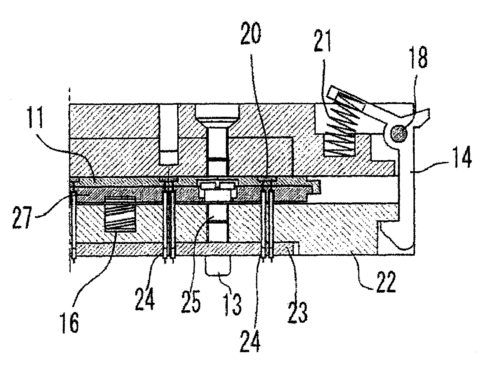
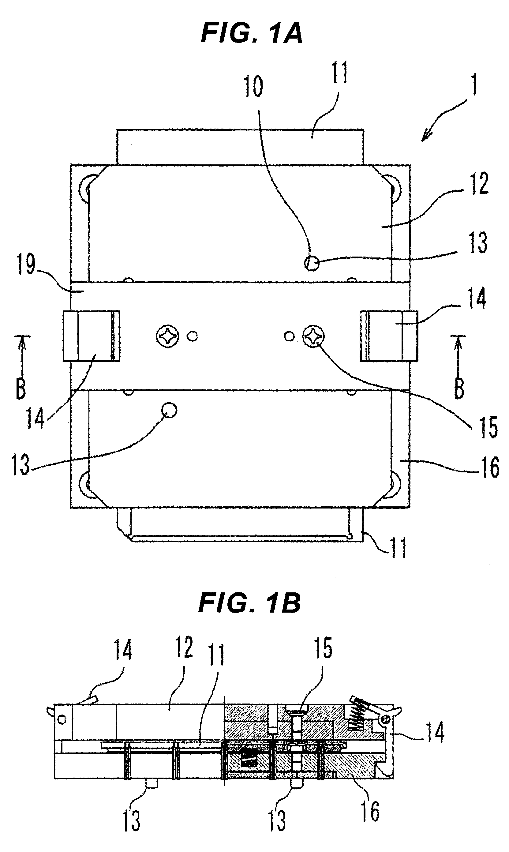
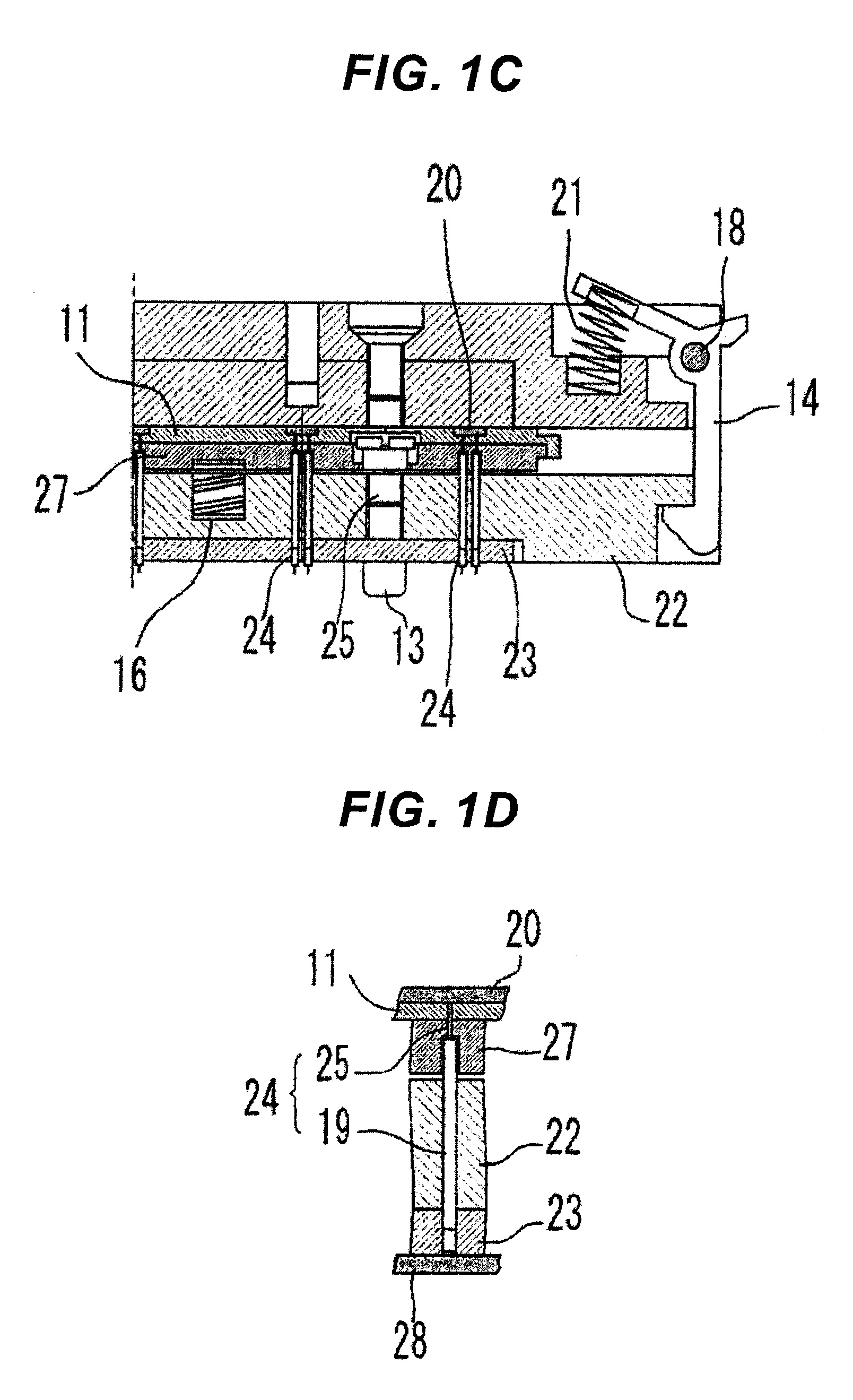
[0028]FIG. 1A to FIG. 1D are diagrams showing an embodiment of a test chip socket according to the present invention. As shown in FIG. 1A, FIG. 1B and FIG. 1C, a test chip socket 1 consists of at least a contact block 16, a tray 11, a cover 12. The contact block 16 is fixed on a tester substrate 28. The tray 11 on which test target chips 20 are mounted is mounted on the contact block 16, and it is fixed to the contact block 16 in a state of being put in between the contact block 16 and the cover 12 by combining the cover 12 with the contact block 16.

[0029]As shown in FIG. 2A, FIG. 2B and FIG. 2C, the tray 11 is a plate type, and for example, formed of injection molded resin. Plurality of mounting sections 29 for respectively mounting one test target chip are formed on the tray 11. Number of the mounting sections 29 for one tray 11 is arbitral, however; number of the test target chips that can be tested at once can be increased by increasing the number of the mounting sections 29.

[00...


PUM


Abstract

A test chip socket comprises a contact block fixed to a tester substrate, a tray mounted to the contact block, the tray having a convex part for positioning test target chips to a plurality of mount positions, and a plurality of probes each of which is held by the contact block and contacts the tester substrate and the test target chip, wherein each probe contacts with a terminal of each test target chip mounted to the mounting position when the tray mounting the plurality of the test target chip is fixed to the contact block.

Description

CROSS REFERENCE TO RELATED APPLICATION[0001]This application is based on Japanese Patent Application 2006-224650, filed on Aug. 21, 2006, the entire contents of which are incorporated herein by reference.BACKGROUND OF THE INVENTION[0002]A) Field of the Invention[0003]This invention relates to a test chip socket.[0004]B) Description of the Related Art[0005]Conventionally a test chip socket is used as a connector for connecting a tester substrate of a test system with a test target chip in a test process of a chip such as a packaged semiconductor integrated circuit.[0006]However, it is impossible to insert a test target chip in a test chip socket and to remove the test target chip from the chip socket on a tester substrate by using an automatic handler. Therefore, in a process of testing a chipped circuit using a test chip socket, handwork to insert or remove the test target chip to or from the test chip socket one by one causes increase in a test cost.[0007]Moreover, a size of a test...

Claims


Application Information

Patent Timeline
Patent Type & Authority Patents(United States)
IPC IPC(8): G01R31/26
CPCG01R31/2886G01R1/0483G01R31/2893
Inventor OHKURA, YOSHIHIRO
Owner YAMAHA CORP
Why Eureka
Try Eureka