Display device

a display device and display technology, applied in the field of display devices, can solve the problems of increased load of clock buses, difficulty in high definition achievement, and increased power consumption,

Active Publication Date: 2010-01-26
JAPAN DISPLAY INC +1
View PDF6 Cites 6 Cited by
  • Summary
  • Abstract
  • Description
  • Claims
  • Application Information

AI Technical Summary

Benefits of technology

[0057]To briefly explain advantageous effects obtained by the typical inventions among inventions disclosed in this specification, they are as follows.
[0058]According to the present invention, it is possible to provide the display device provided with the drive circuit having the CMOS shift register which is constituted of a simple CMOS circuit.

Problems solved by technology

Along with the development of high definition, as shown in FIG. 15, the CMOS shift register has a drawback that the number of transistor elements is increased thus giving rise to a drawback that the achievement of high definition is difficult.
Further, p-type MOS transistors (PM1, PM2) and n-type MOS transistors (NM1, NM2) shown in FIG. 15 are configured such that a gate is directly connected to a clock bus through which a clock (CLK) and an inverted clock (CLKB) are transmitted and hence, a load of the clock bus is increased thus giving rise to a drawback that the power consumption is increased.
Further, the p-type MOS transistors (PM1, PM2) and the n-type MOS transistors (NM1, NM2) shown in FIG. 15 are operated for every clock signal and hence, the transistor is remarkably deteriorated thus giving rise to a drawback with respect to the reliability thereof in a high speed operation.

Method used


Image

  • Display device
  • Display device
  • Display device

Examples


Embodiment Construction

[0074]Hereinafter, embodiments of the present invention are explained in detail in conjunction with drawings.

[0075]Here, in all drawings for explaining the embodiments, parts having identical functions are given same symbols and their repeated explanation is omitted.

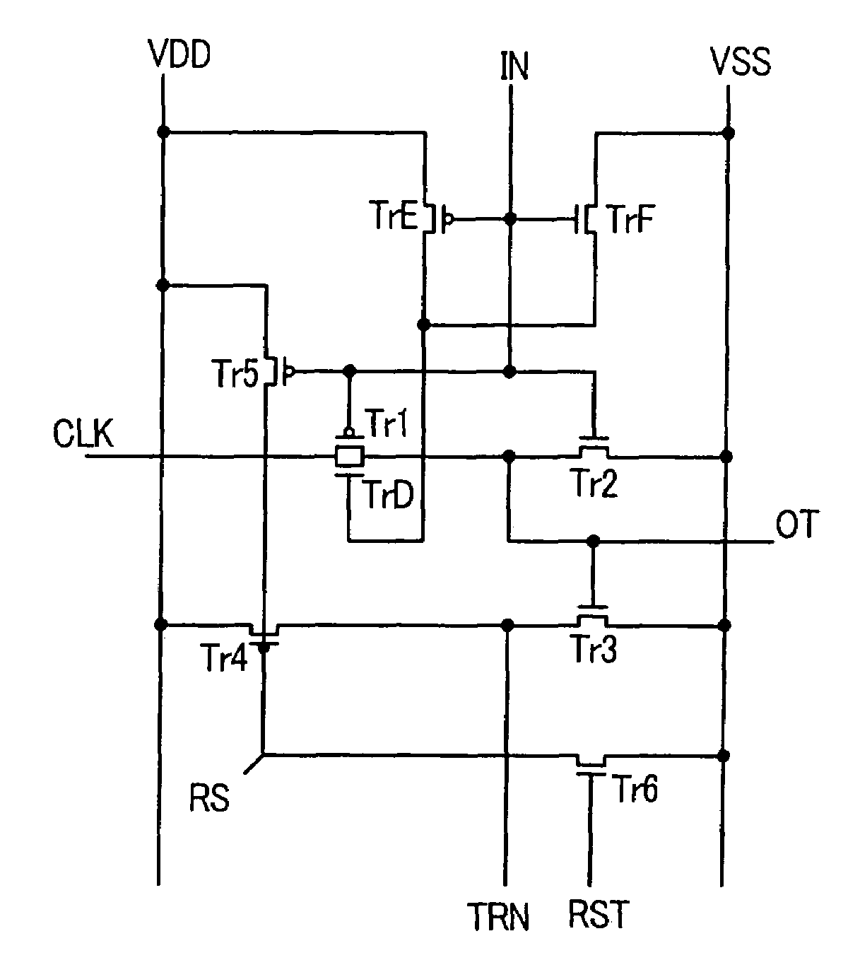
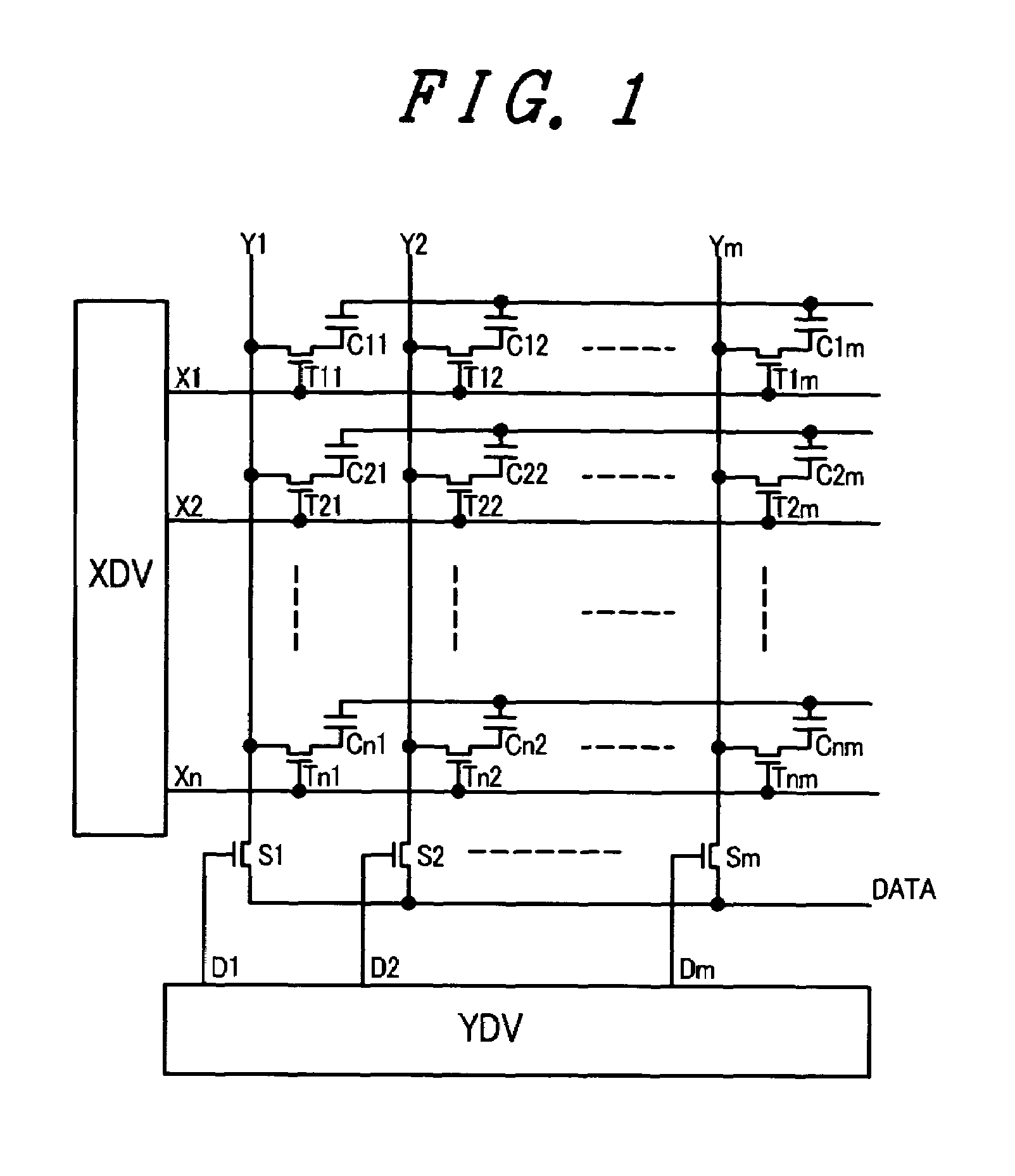
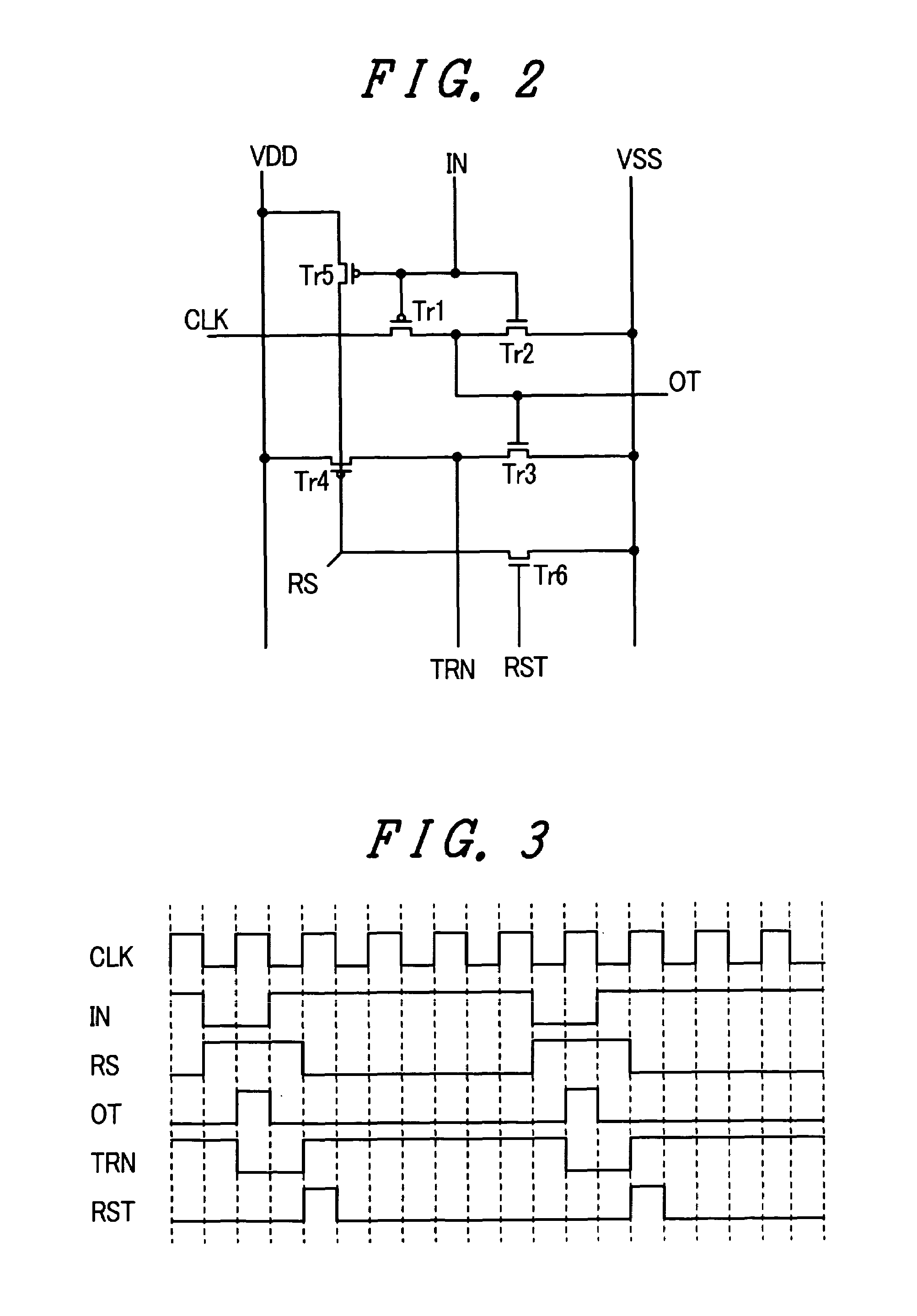
[0076]FIG. 1 is a circuit diagram showing an equivalent circuit of an active matrix type liquid crystal display device of an embodiment of the present invention.

[0077]As shown in FIG. 1, the active matrix type liquid crystal display device of the embodiment includes, on a liquid crystal surface of one of a pair of substrates which are arranged to face each other with a liquid crystal therebetween, n-pieces of scanning lines (X1, X2, . . . Xn) which extend in the x direction and m pieces of video lines (Y1, Y2, . . . Ym) which extend in the y direction.

[0078]Regions which are surrounded by the scanning lines (also referred to as gate lines) and the video lines (also referred to as drain lines) constitute pixel regions. Ea...


PUM


Abstract

The present invention relates to a display device, and more particularly to a display device which includes a drive circuit having a CMOS shift register which is constituted of a CMOS circuit. The display device includes: a plurality of pixels; and a drive circuit, wherein the drive circuit includes a shift register that includes n(n≧2) basic circuits connected vertically in multiple rows, the basic circuit includes a first transistor having a first electrode to which a clock is applied, and a second transistor of a second conductive type which is different from the first transistor of the first conductive type in a conductive type and has a second electrode thereof connected to a second electrode of the first transistor and has a second power source voltage applied to a first electrode thereof, an input signal is applied to a control electrode of the first transistor and a control electrode of the second transistor, and the second electrode of the first transistor is connected to a scanning circuit output terminal.

Description

CROSS-REFERENCE TO RELATED APPLICATIONS[0001]The disclosure of Japanese Patent Application No. P2005-281040 filed on Sep. 28, 2005 including the claims, the specification, the drawings and the abstract is incorporated herein by reference in its entirety.BACKGROUND OF THE INVENTION[0002]1. Field of the Invention[0003]The present invention relates to a display device, and more particularly to a display device which includes a drive circuit having a CMOS shift register which is constituted of a CMOS circuit.[0004]2. Description of the Related Art[0005]In general, in an active matrix liquid crystal display device which uses thin film transistors (TFT: Thin Film Transistor) as active elements, for example, a shift register circuit is used for sequentially applying a selective scanning voltage to scanning lines.[0006]As the shift register circuit, there have been known a CMOS shift register which is constituted of a CMOS (Complementary Metal Oxide Semiconductor) (see following Patent Docu...

Claims


Application Information

Patent Timeline
Patent Type & Authority Patents(United States)
IPC IPC(8): G09G3/36
CPCG09G3/3677G11C19/184G11C19/28G09G2310/0286G09G2330/021
Inventor NAKAO, TAKAYUKISATO, HIDEOMAKI, MASAHIRO
Owner JAPAN DISPLAY INC
Why Eureka
Try Eureka