Transmission device
a transmission device and output signal technology, applied in the direction of logic circuits, pulse techniques, reliability increasing modifications, etc., can solve the problems of difficulty in finely adjusting the output amplitude, the variations of the output signals txop and txon do not meet the requirements specified by the various standards, and the transmission device cannot concurrently satisfy various requirements
- Summary
- Abstract
- Description
- Claims
- Application Information
AI Technical Summary
Benefits of technology
Problems solved by technology
Method used
Image


Examples
first embodiment
1. First Embodiment
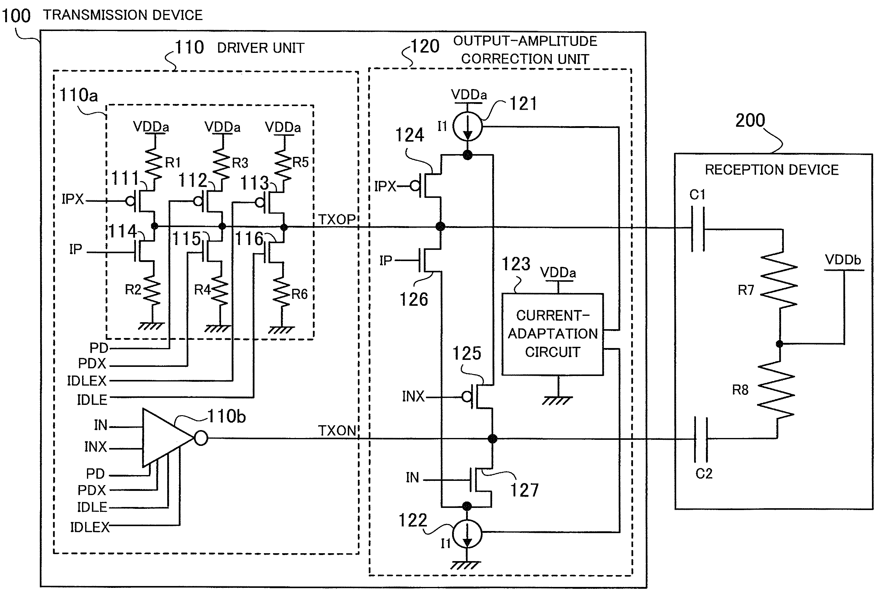
[0078]FIG. 1 is a diagram illustrating circuit constructions of a transmission device and a reception device according to the first embodiment. The transmission device 100 according to the first embodiment comprises a driver unit 110 and an output-amplitude correction unit 120. The driver unit 110 generates output signals TXOP and TXON, and the output-amplitude correction unit 120 corrects the amplitudes of the output signals TXOP and TXON (i.e., the output amplitudes of the driver unit 110).
[0079]The driver unit 110 comprises two driver circuits 110a and 110b, makes a resistance division of the power-supply voltage VDDa, and outputs the output signals TXOP and TXON from the driver circuits 110a and 110b, respectively. In FIG. 1, the input signals IP, IPX, IN, and INX are main signals, and the other input signals PD, PDX, IDLE, and IDLEX are signals used for generating a common-mode voltage and an idle voltage by resistance division.
[0080]The driver circuit 110a i...
second embodiment
2. Second Embodiment
[0144]The transmission device 100 according to the first embodiment suppresses the variations in the output amplitudes caused by the variations in the power-supply voltage VDDa, by generating such correction current I1 that the output amplitudes are increased in correction by an amount which increases with decrease in the power-supply voltage VDDa. On the other hand, the variations in the output amplitudes caused by the variations in the power-supply voltage VDDa can be suppressed by generating such correction current I1 that the output amplitudes are decreased in correction by an amount which increases with increase in the power-supply voltage VDDa.
[0145]The second embodiment is explained in detail below.
[0146]FIG. 8 is a diagram illustrating circuit constructions of a transmission device and a reception device according to the second embodiment. In FIG. 8, the same elements as the elements in the transmission device 100 according to the first embodiment respect...
third embodiment
4. Third Embodiment
[0186]The third embodiment is explained in detail below.
[0187]FIG. 17 is a diagram illustrating a circuit construction of a transmission device according to the third embodiment. In FIG. 17, the same elements as the elements in FIG. 1 respectively bear the same reference numbers. Therefore, the explanations on the same elements are not repeated unless necessary.
[0188]The transmission device 300 illustrated in FIG. 17 comprises a driver unit 310 and an output-amplitude correction unit 320, and realizes the functions of pre-emphasis and de-emphasis according to PCI Express. The input signals (as the boost signals) IBP, IBPX, IBN, and IBNX, as well as the input signals (as the main signals) IP, IPX, IN, and INX, are inputted into the driver unit 310 and the output-amplitude correction unit 320 in the transmission device 300 for generating and correcting pre-emphasis and de-emphasis signals.
[0189]The driver unit 310 comprises two driver circuits 310a and 310b. The dri...
PUM
 Abstract
Description
Claims
Application Information