Method of reducing electro-static discharge (ESD) from conductors on insulators

a technology of electrostatic discharge and conductor, which is applied in the direction of emergency protective arrangements for limiting excess voltage/current, instruments, and record information storage, etc., can solve the problems of insufficient design of certain electronic devices in the marketplace low tolerance to esd, and inability to effectively deal with esd. to achieve the effect of reducing the amount of electrostatic charge carried

Inactive Publication Date: 2010-03-16
OPSEC SECURITY GROUP
View PDF44 Cites 13 Cited by
  • Summary
  • Abstract
  • Description
  • Claims
  • Application Information

AI Technical Summary

Benefits of technology

[0006]It is an object of the present invention to eliminate or reduce the amount of electrostatic charge carried or stored on a conductive component of an insulating device that interfaces with electronic devices, persons or objects.
[0008]In accordance with an embodiment of the present invention, the resistance of the conductive (or metal) layer on the non-conductive carrier is increased by disrupting the conductivity path. Physical breaks are introduced in the conductive layer by removing portions of the conductive layer or by selective application of a conductive layer.
[0009]In accordance with an embodiment of the present invention, a non-conductive carrier comprises a conductive component that is fragmented into a plurality of sections to disrupt the conductive component's conductive path. Each section is isolated from other sections so as to minimize a charge accumulated in one section from combining with the charge accumulated in another section, thereby minimizing any potential electrostatic discharge. Alternatively, each section is isolated from other sections Such that a charge accumulated in one section cannot combine with the charge accumulated in another section, thereby minimizing any potential electrostatic discharge from the conductive component of the carrier.
[0010]In accordance with an embodiment of the present invention, a method of reducing electrostatic discharge from a conductive layer on a non-conductive carrier comprises the steps of fragmenting the conductive layer into a plurality of sections to disrupt the conductive layer's conductive path; and isolating each section from other sections such that a charge accumulated in one section cannot combine with the charge accumulated in another section, thereby minimizing any potential electrostatic discharge from the conductive component of the carrier. Alternatively, each section being isolated from other sections so as to minimize a charge accumulated in one section from combining with the charge accumulated in another section, thereby minimizing any potential electrostatic discharge.
[0011]In accordance with an embodiment of the present invention, a method of reducing electrostatic discharge from a conductive layer on a non-conductive carrier comprises the steps of forming a fragmented conductive layer comprising a plurality of sections to disrupt the conductive layer's conductive path; and isolating each section from other sections such that a charge accumulated in one section cannot combine with the charge accumulated in another section, thereby minimizing any potential electrostatic discharge from the metal component of the carrier. Alternatively, each section being isolated from other sections so as to minimize a charge accumulated in one section from combining with the charge accumulated in another section, thereby minimizing any potential electrostatic discharge.
[0012]In accordance with an embodiment of the present invention, a metalized article is divided into a plurality of sections to disrupt the metalized article's conductive path. Each section being isolated from other sections so as to minimize a charge accumulated in one section from combining with the charge accumulated in another section, thereby minimizing any potential electrostatic discharge. Preferably, the metalized article comprises a non-conducting backing support, which is an integral part of the metalized article.

Problems solved by technology

If the charged insulator, containing the conductor, is inserted into or passed close to an electronic device these induced charges in the conductor can transfer into or onto the electronic device and cause disruption of the functions of the electronic device or nearby electronic devices.
However, certain electronic devices in the marketplace are not adequately designed to effectively deal with the ESD and have low tolerance to ESD.
If the ESD energy is not channeled properly, then it can disrupt the operation of the electronic device.

Method used


Image

  • Method of reducing electro-static discharge (ESD) from conductors on insulators
  • Method of reducing electro-static discharge (ESD) from conductors on insulators
  • Method of reducing electro-static discharge (ESD) from conductors on insulators

Examples


Embodiment Construction

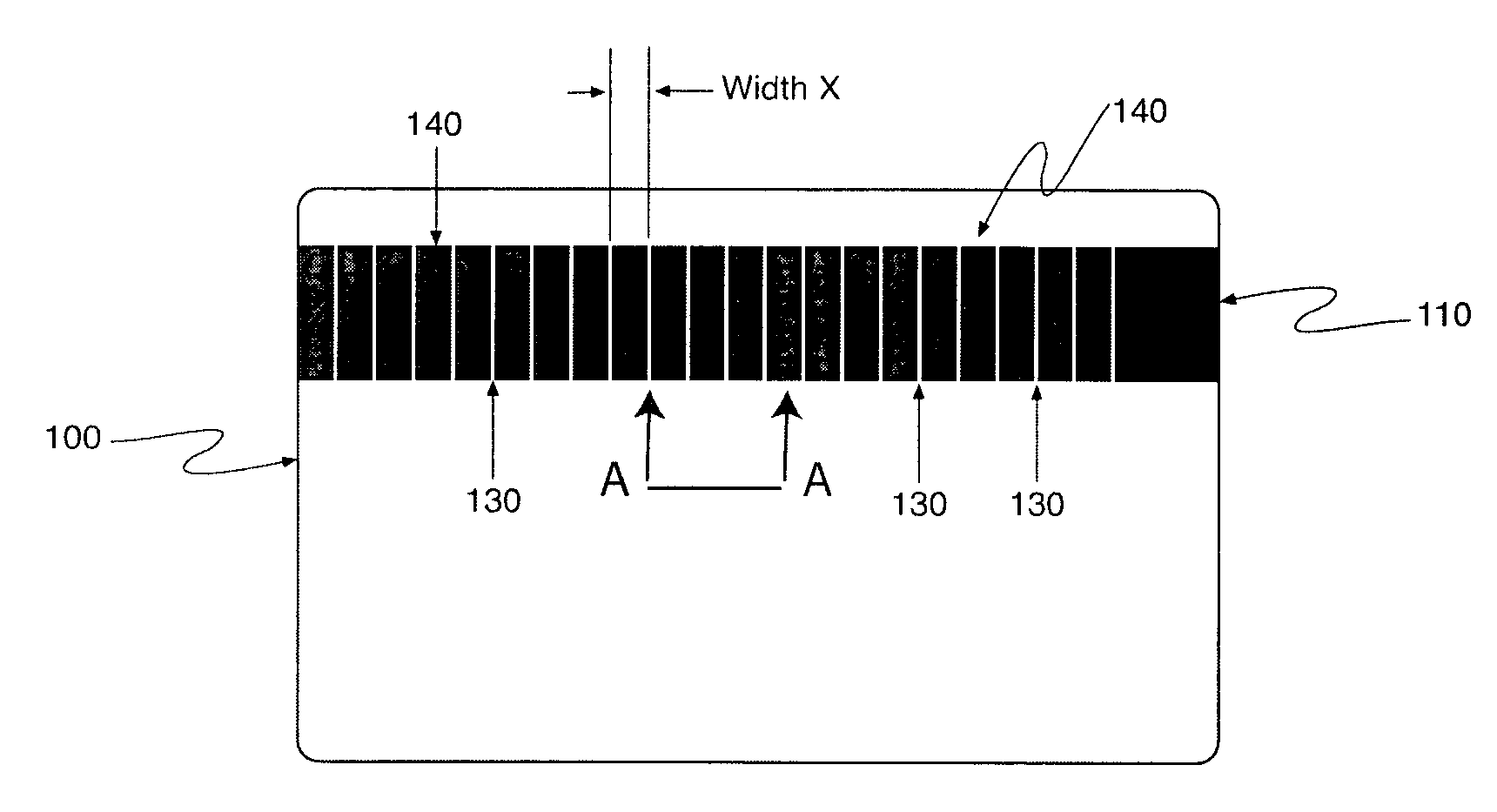
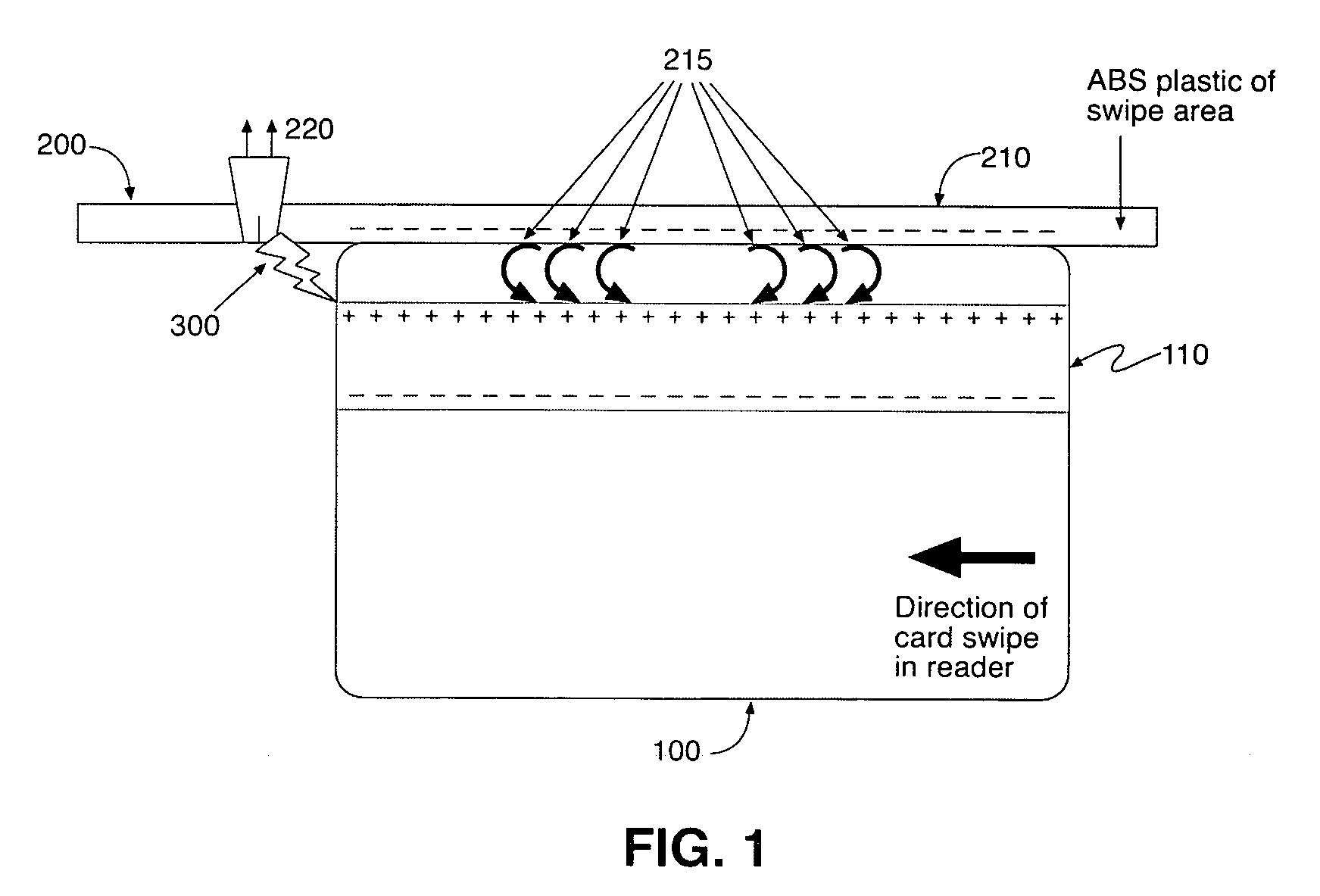
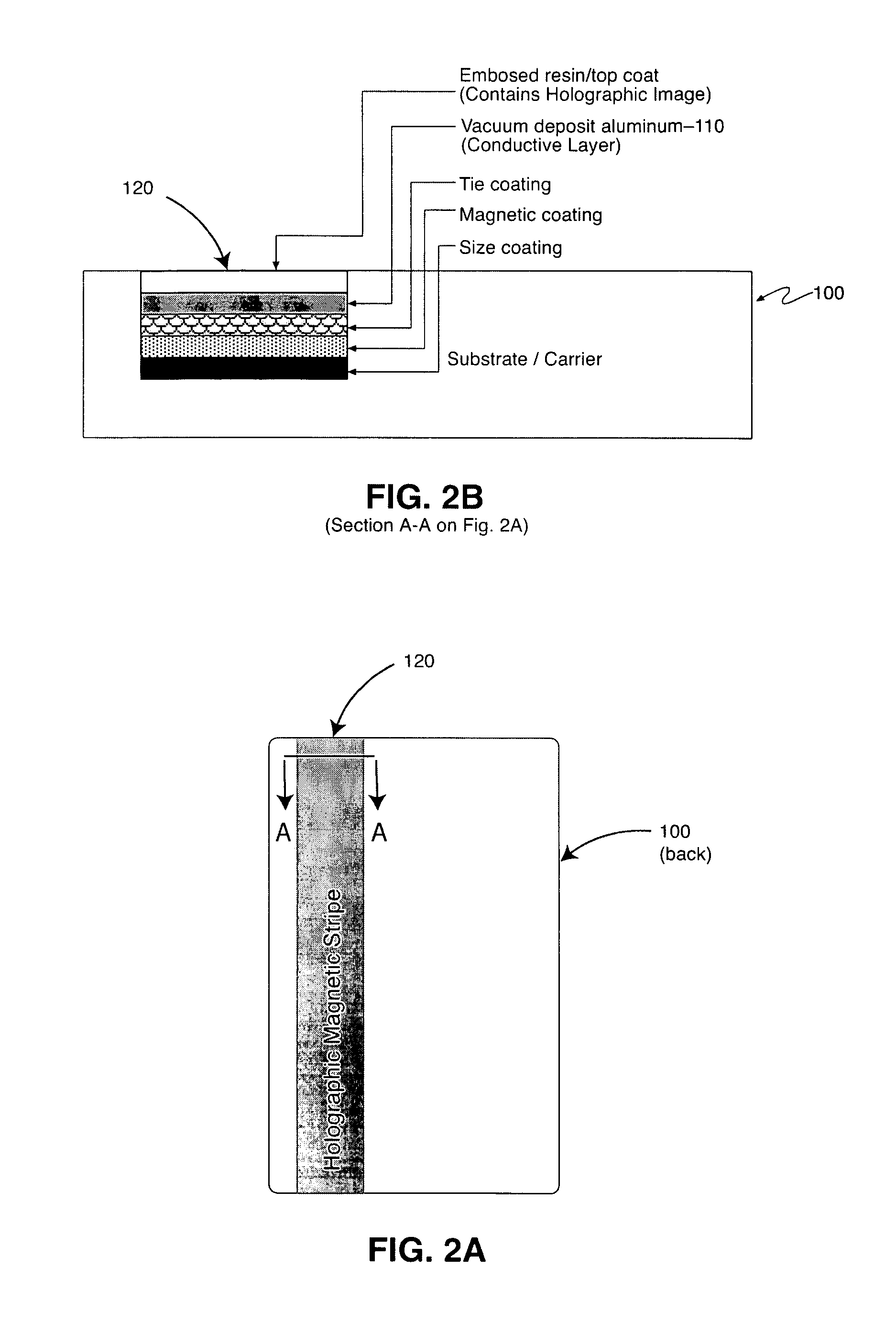
[0027]There are many examples of insulator devices that carry conducting components that can be charged and then discharged into an electronic device. The inventive method is applicable to reduce or eliminate ESD from a conductive component 110 on an insulator 100. Turning now to FIG. 1, the inventive method is described as applied to a polyvinyl chloride (PVC) plastic card (insulator) 100 with a metal conductive coated magnetic stripe (metal component) 110 to reduce or eliminate ESD from a metal component 110 on an insulator 100. A PVC plastic card 100 carrying a metalized magnetic stripe (“mag stripe”) 110 is inserted into a magnetic stripe card reader 200, such as a point of sale (POS) terminal 200, where ESD 300 from the metalized magnetic stripe 110 into the POS terminal 200 can disrupt the operation of the POS terminal 200. The following descriptions describe how a conductor or conductive layer 110 on a non-conducting carrier 100 can hold charge that can disrupt electronic dev...


PUM


Abstract

A non-conductive carrier having a conductive component comprising a plurality of sections to disrupt the conductive component's conductive path. Each section is isolated from other sections such that a charge accumulated in one section cannot combine with the charge accumulated in another section, thereby minimizing any potential electrostatic discharge from the carrier.

Description

RELATED APPLICATION[0001]This application claims priority benefit of provisional application Ser. Nos. 60 / 776,717, 60 / 776,720 and 60 / 776,718, all filed Feb. 24, 2006, each of which is incorporated by reference in its entirety.BACKGROUND OF THE INVENTION[0002]Electrostatic charge can be built up and held on an insulator by many methods. A common method is by triboelectric generation of the charge by moving two different materials in contact with each other. As shown in FIG. 1, opposite charges (Positive + and Negative − charges) can build up on each material depending upon their ability to donate or capture electrons that are freed up due to the frictional forces generated during the movement of one material against the other. The charge that builds up on either material is called a static charge (not moving) or electro static charge. It remains on the material for some period of time depending upon the environment with which the material is in contact during the charge holding perio...

Claims


Application Information

Patent Timeline
Patent Type & Authority Patents(United States)
IPC IPC(8): G06K19/06
CPCG06K19/06196G03H1/0252G11B5/80G11B5/72G03H2250/12G03H1/0244G11B5/7262G06K3/00G11C11/00G11C13/00G11C7/02
Inventor HYNES, JOHNKAWAND, JOHNO'BOYLE, LILYSADASIVAN, SUNDARVINCITORE, LEONARDOD'AMATO, SALVATORE F.
Owner OPSEC SECURITY GROUP
Why Eureka
Try Eureka