TFT-LCD pixel structure and manufacturing method thereof

a technology of liquid crystal display and thin film transistor, which is applied in the direction of optics, radio frequency control devices, instruments, etc., can solve the problems of reducing the production volume and yield of tft-lcd, complication of the manufacturing process, and complicated other processes in manufacturing tft-lcd, so as to reduce the number of masks, reduce the cost of array process and seizing time, and improve production volume and yield

Active Publication Date: 2010-03-30
BEIJING BOE OPTOELECTRONCIS TECH CO LTD +1
View PDF2 Cites 3 Cited by
  • Summary
  • Abstract
  • Description
  • Claims
  • Application Information

AI Technical Summary

Benefits of technology

[0011]The TFT-LCD pixel structure and the manufacturing method thereof according to the embodiments of the present invention can reach the following advantages.
[0012]A second insulating layer is deposited during the first photolithography process so that the pixel structure can be planarized, which provides process tolerance for subsequent processes. In addition, a portion of the transparent pixel electrode is also used as the drain electrode of the TFT, which can avoid the problem about contact resistance.
[0013]As compared with the conventional method, two masks can be used to manufacture a TFT-LCD pixel structure, the number of masks can be decreased, the cost for the array process and the seizing time can be reduced, and the production volume and yield can be improved. In addition, since the number of the masks and also exposure processes is decreased, the complication of the process can be reduced, the process tolerance can be increased, and the production volume and yield can be improved.

Problems solved by technology

However, decrease of the times of photolithography with a mask may render other processes in manufacturing a TFT-LCD complicated and may even make impossible to carry out such processes.
The fabrication of these portions is the key for manufacturing a TFT-LCD, which, in practice, imposes rigorous requirements on etching selectivity and the photolithography process and further brings complication to the manufacturing process.

Method used


Image

  • TFT-LCD pixel structure and manufacturing method thereof
  • TFT-LCD pixel structure and manufacturing method thereof
  • TFT-LCD pixel structure and manufacturing method thereof

Examples


Embodiment Construction

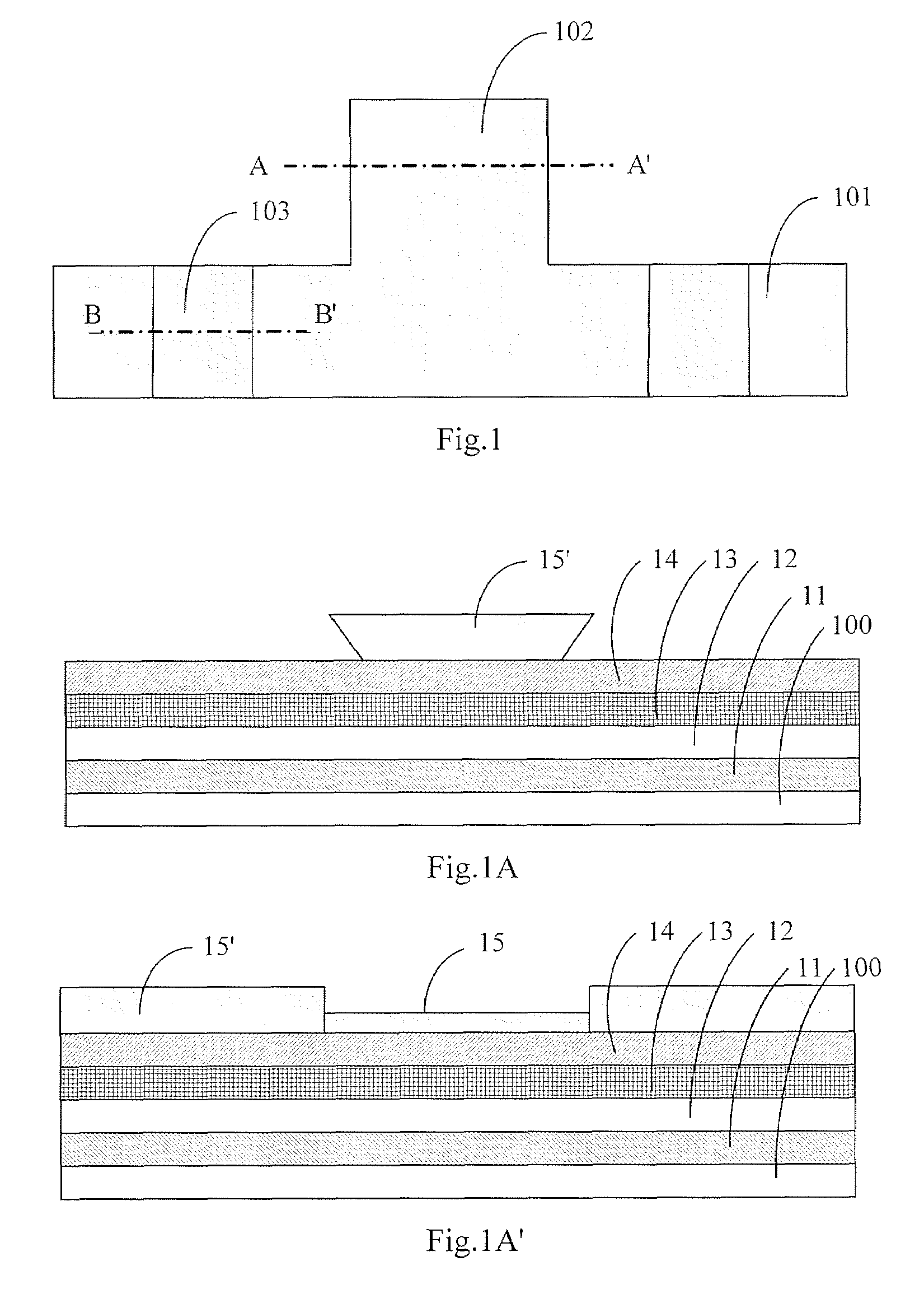
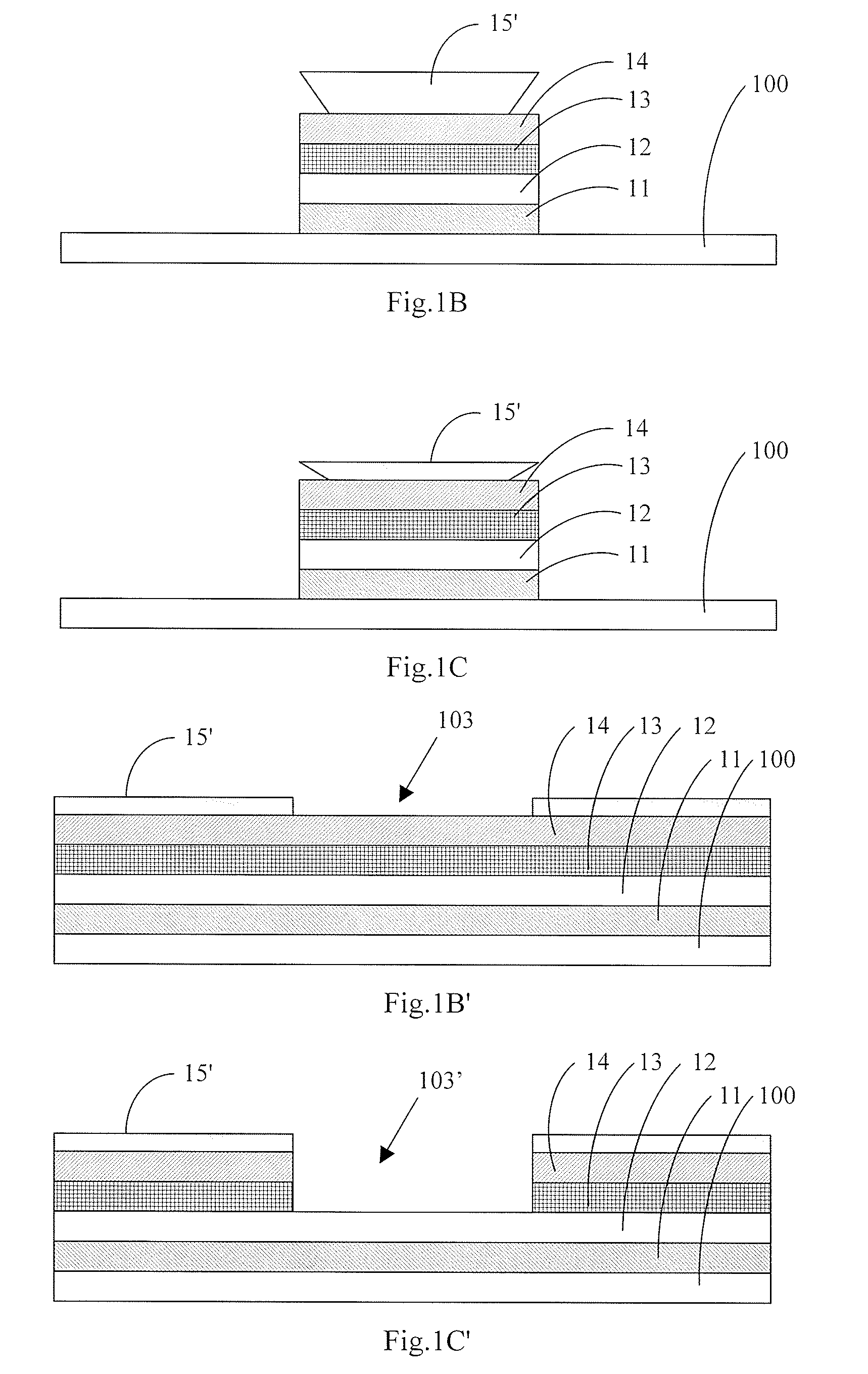
[0035]Embodiments of the present invention are described below in detail with reference to the accompanying drawings. In this disclosure, a gray tone mask may be a mask with a transparence region, a translucence region and a blocked region, and the translucence region can be obtained with slits that can diffract light, a translucent material of low transmissivity and the like, thus a gray tone mask also comprises a half tone mask.

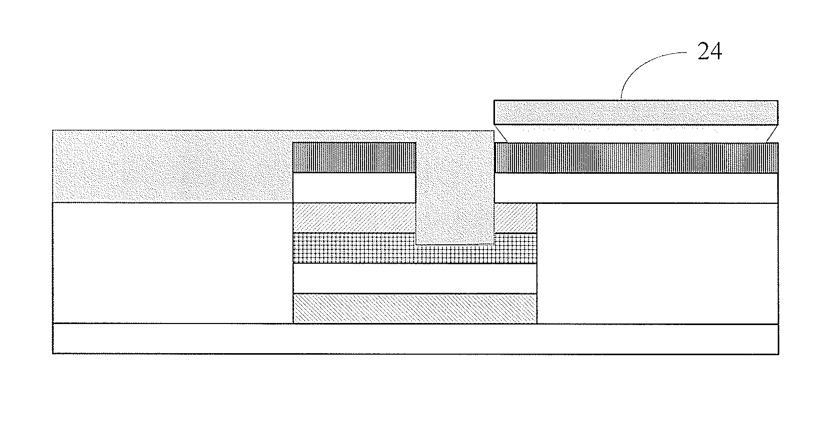
[0036]FIG. 1 is a top view showing a pattern after a first photolithography is carried out with a first gray tone mask, FIG. 1A is a cross-sectional view along line A-A′ in FIG. 1, and FIG. 1A′ is a cross-sectional view along line B-B′ in FIG. 1. As shown in FIGS. 1, 1A, and 1A′, a gate conductive layer 11, a first insulating layer 12, a semiconductor layer 13, and a doped semiconductor layer 14 are deposited in sequence on a substrate 100, a photoresist film is applied on the resultant layer structure, and an exposure process with the first gray tone mask ...


PUM


Abstract

A thin film transistor liquid crystal display (TFT-LCD) pixel structure comprising: a gate line and a gate electrode formed on a substrate; a first insulating layer, a semiconductor layer, and a doped semiconductor layer formed sequentially on the gate electrode and the gate line, wherein an isolating groove is formed above the gate line which disconnects the semiconductor layer on the gate line; a second insulating layer covering the isolating groove and a portion of the substrate where the gate line and the gate are not formed; a pixel electrode formed on the second insulating layer, wherein the pixel electrode is integral with a drain electrode and is connected with the doped semiconductor layer on the gate electrode at a place where the drain electrode is formed; a source electrode, which is a portion of a data line, formed on the doped semiconductor layer; and a channel formed between the source electrode and the drain electrode.

Description

FIELD OF THE INVENTION[0001]The present invention relates to a method of manufacturing a thin film transistor liquid crystal display (TFT-LCD) and the TFT-LCD thus manufactured.BACKGROUND OF THE INVENTION[0002]At present, a liquid crystal displays (LCD) exemplified by a TFT-LCD has become one very important type of flat panel displays and has attracted extensive attention. During manufacture of a TFT-LCD, efforts have been made to adopt a more advanced manufacturing method, simplify producing process, and reduce production cost. Among the others, simplification of process and the reduction of production cost for each device of a TFT-LCD directly lead to the simplification of manufacturing process and the reduction of production cost of the whole TFT-LCD.[0003]A LCD generally comprises an upper substrate and a lower substrate which are joined together by a seal agent. Electrodes are formed on the upper and lower substrates, and liquid crystal material is filled between the two substr...

Claims


Application Information

Patent Timeline
Patent Type & Authority Patents(United States)
IPC IPC(8): H01L21/00
CPCH01L27/1214G02F2001/133357G02F2001/136231G02F2001/13625G02F2001/136236G02F1/133357G02F1/136231G02F1/136236G02F1/13625H01L27/1288
Inventor QIU, HAIJUNWANG, ZHANGTAOMIN, TAE YUP
Owner BEIJING BOE OPTOELECTRONCIS TECH CO LTD
Why Eureka
Try Eureka