Touch module

a technology of touch module and lithographic etching process, which is applied in the direction of instruments, contacts, contact surface shape/structure, etc., can solve the problems of increasing the total manufacturing cost, increasing the risk of chemical solutions harmful to human health, and high cost of optical mask design and lithographic and etching equipment, so as to reduce the manufacturing cost, improve the ratio of good products, and save the effect of optical mask design

Active Publication Date: 2014-06-19
LIN CHIH CHUNG
View PDF2 Cites 3 Cited by
  • Summary
  • Abstract
  • Description
  • Claims
  • Application Information

AI Technical Summary

Benefits of technology

[0012]It is therefore a primary object of the present invention to provide a touch module, which is manufactured without optical mask and lithographic and etching process so that the cost for the optical mask design and the lithographic and etching process is saved to lower the manufacturing cost.
[0013]It is a further object of the present invention to provide a touch module, which is manufactured without using optical glue layer to adhere the transparent substrates to each other. Therefore, the problem existing in the conventional touch panel that the transparent substrates often fail to fully attach to each other is eliminated. Therefore, the ratio of good products is increased.
[0014]To achieve the above and other objects, the touch module of the present invention includes a transparent substrate, a shield layer, a touch electrode layer, a transparent insulation layer and a lead layer. The transparent substrate has a first side and a second side opposite to the first side. The shield layer is coated on an edge of the second side of the transparent substrate. The touch electrode layer is disposed on the second side of the transparent substrate and coated on the other side of the shield layer, which side is distal from the transparent substrate. The transparent insulation layer is disposed on the other side of the touch electrode layer, which side is distal from the shield layer. The transparent insulation layer is formed with at least one through hole on the touch electrode layer. The lead layer is disposed on the other side of the transparent insulation layer, which side is distal from the touch electrode layer. The lead layer is formed with a conduction section positioned in the through hole in electrical connection with the touch electrode layer. Accordingly, the lead layer can directly electrically connect with the touch electrode layer through the through hole of the transparent insulation layer. In this case, the cost for the optical mask design and the lithographic and etching processes can be saved. Moreover, the problem existing in the conventional touch panel that the first and second transparent substrates often fail to fully attach to each other is eliminated. Therefore, the ratio of defective products is lowered.

Problems solved by technology

The cost for the optical mask and the lithographic and etching equipment is quite high so that the total manufacturing cost is inevitably increased.
Moreover, the developer and etching liquid used in the lithography and etching processes are both chemical solutions harmful to human health.
Therefore, the developer and etching liquid not only seriously threaten the health of the workers in the working site, but also lead to serious pollution of the ecological environment.
This will cause defective products.

Method used


Image

  • Touch module
  • Touch module
  • Touch module

Examples


Embodiment Construction

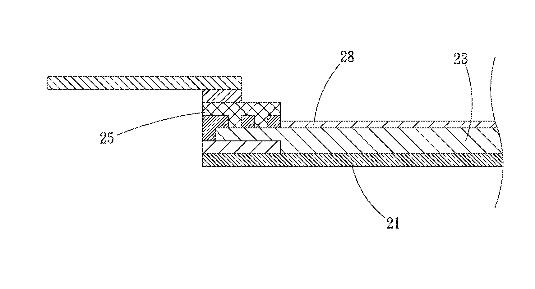
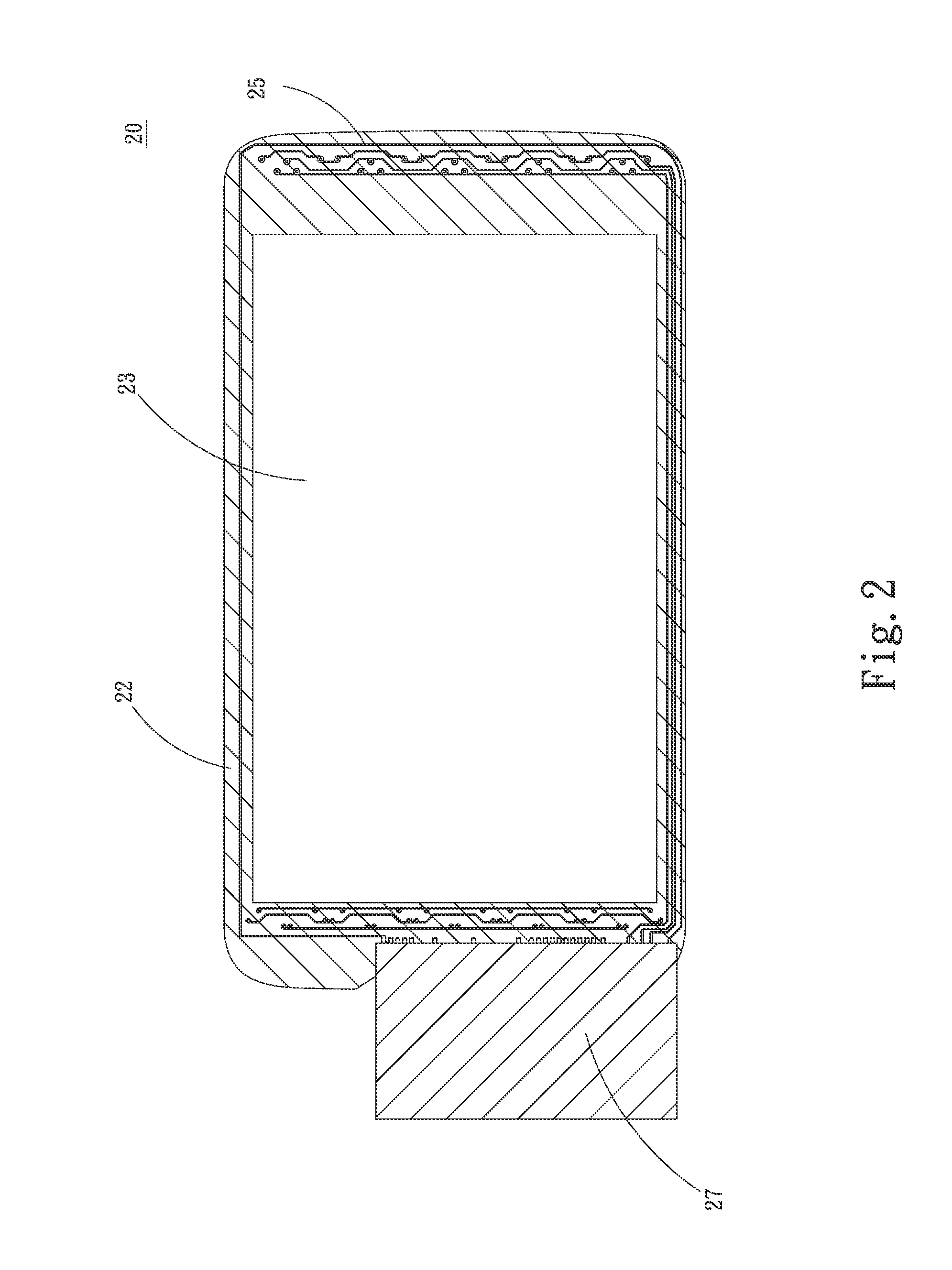
[0020]Please refer to FIGS. 2 and 3. FIG. 2 is a plane assembled view of a first embodiment of the present invention. FIG. 3 is a sectional assembled view of the first embodiment of the present invention. According to the first embodiment, the touch module 20 of the present invention includes a transparent substrate 21, a shield layer 22, a touch electrode layer 23, a transparent insulation layer 24 and a lead layer 25. The transparent substrate 21 has a first side 211 and a second side 212 opposite to the first side 211. In this embodiment, the transparent substrate 21 is made of a material, which is, but not limited to, glass for illustration purposes only. Alternatively, the material of the transparent substrate 10 can be selected from a group consisting of polyethylene terephthalate (PET), polycarbonate (PC), polyethylene (PE), polyvinyl chloride (PVC), polypropylene (PP), polystyrene (PS), polymethylmethacrylate (PMMA) and cyclo olefin copolymer (COC).

[0021]The shield layer 22 ...


PUM


Abstract

A touch module includes a transparent substrate, a shield layer, a touch electrode layer, a transparent insulation layer and a lead layer. The shield layer is coated on the transparent substrate. The touch electrode layer is coated on both the transparent substrate and the shield layer. The transparent insulation layer is disposed on the touch electrode layer and formed with at least one through hole. The lead layer is disposed on the transparent insulation layer and formed with a conduction section positioned in the through hole in electrical connection with the touch electrode layer. Therefore, the lead layer can directly electrically connect with the touch electrode layer through the through hole of the transparent insulation layer. Accordingly, the cost for the optical mask design and the lithographic and etching processes can be saved and the problem that the transparent substrates often fail to fully attach is eliminated.

Description

[0001]This application claims the priority benefit of Taiwan patent application number 101148211 filed on Dec. 19, 2012.BACKGROUND OF THE INVENTION[0002]1. Field of the Invention[0003]The present invention relates generally to a touch module, and more particularly to a touch module in which the wiring structure is changed.[0004]2. Description of the Related Art[0005]Along with the rapid development of information techniques and communication networks, various personal electronic information products have been more and more popularly used. To go with the tide, various touch panels have bee rapidly developed and applied to the electronic products. According to the sensing principle, the current touch panels can be mainly classified into resistive touch panels, capacitive touch panels, electromagnetic touch panels and optical touch panels. The capacitive touch panel structures have the advantages of dustproof, fireproof and high-resolution performances and are thus widely used. The wor...

Claims


Application Information

Patent Timeline
Patent Type & Authority Applications(United States)
IPC IPC(8): H01H1/06
CPCG06F3/04164G06F3/0443G06F2203/04107
Inventor LIN, CHIH-CHUNG
Owner LIN CHIH CHUNG
Why Eureka
Try Eureka