Gallium nitride based light emitting diode

a technology of gallium nitride and light-emitting diodes, which is applied in the manufacturing of semiconductor/solid-state devices, semiconductor devices, electrical devices, etc., can solve the problems of reducing the characteristics and reliability of the diodes, the overall manufacturing process becomes complex, and the diodes are difficult to manufacture. achieve the effect of preventing defective adhesion, simplifying the overall manufacturing process, and enhancing the adhesive performance between the protective film and the electrod

Active Publication Date: 2010-03-30
SAMSUNG ELECTRONICS CO LTD
View PDF7 Cites 19 Cited by
  • Summary
  • Abstract
  • Description
  • Claims
  • Application Information

AI Technical Summary

Benefits of technology

[0019]An advantage of the present invention is that it provides a GaN-based LED in which a transparent electrode and a protective film are simultaneously formed by using a transparent layer composed of an indium oxide without a separate etching process. Therefore, the overall manufacturing process is simplified, and simultaneously, the adhesive performance between the protective film and an electrode is enhanced, thereby preventing defective adhesion.
[0020]Another advantage of the invention is that it provides a method of manufacturing the above-described GaN-based LED.
[0021]Additional aspect and advantages of the present general inventive concept will be set forth in part in the description which follows and, in part, will be obvious from the description, or may be learned by practice of the general inventive concept.
[0022]According to an aspect of the invention, a GaN-based LED comprises a substrate; an an-type GaN layer formed on the substrate; an active layer formed on a predetermined region of the n-type GaN layer; a p-type GaN layer formed on the active layer; a transparent electrode formed on the p-type GaN layer; a p-electrode formed on the transparent electrode; an n-type electrode formed on the n-type GaN layer on which the active layer is not formed; and a protective film formed on a resulting structure between the transparent electrode and the n-type electrode, the protective film being composed of a plasma-oxidized transparent layer.
[0023]According to another aspect of the invention, the protective film is formed is the resulting structure between the transparent electrode and the n-type electrode and may be composed of a transparent layer subjected to an ashing process.
[0024]According to a further aspect of the invention, the transparent layer is composed of a compound formed by adding one or more elements, selected from a group consisting of tin, zinc, magnesium, copper, silver, and aluminum, into an indium oxide. The elements are added by 1 to 30 wt % of the overall compound.

Problems solved by technology

Therefore, the overall manufacturing process becomes complex.
As described above, in the method of manufacturing a GaN-based LED according to the related art, the overall manufacturing process is complex.
Further, since a SiO2 or SiN film used as the protective film has poor adhesion performance with the electrodes, that is, the transparent electrode 120, the p-electrode 140, and the n-electrode 130, defective adhesion (for example, the film can be peeled off) occurs, thereby reducing characteristics and reliability of the diode.

Method used


Image

  • Gallium nitride based light emitting diode
  • Gallium nitride based light emitting diode
  • Gallium nitride based light emitting diode

Examples


Embodiment Construction

[0041]Reference will now be made in detail to the embodiments of the present general inventive concept, examples of which are illustrated in the accompanying drawings, wherein like reference numerals refer to like elements throughout. The embodiments are described below in order to explain the present general inventive concept by referring to the figures.

[0042]Hereinafter, a GaN-based LED and a method of manufacturing the same according to an embodiment of the present invention will be described in detail with reference to the accompanying drawings.

[0043]Structure of GaN-Based LED

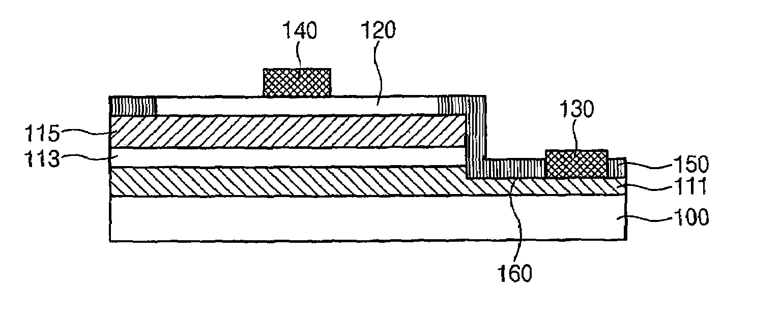
[0044]Referring to FIG. 2, the structure of a GaN-based LED according to an embodiment of the invention will be described in detail.

[0045]As shown in FIG. 2, the GaN-based LED includes a buffer layer (not shown), an n-type GaN layer 111, an active layer 113, and a p-type GaN layer 115, which are sequentially laminated on an optically-transparent substrate 100, thereby forming a light emitting structure.

[004...


PUM


Abstract

A GaN-based LED comprises a substrate; an an-type GaN layer formed on the substrate; an active layer formed on a predetermined region of the n-type GaN layer; a p-type GaN layer formed on the active layer; a transparent electrode formed on the p-type GaN layer; a p-electrode formed on the transparent electrode; an n-type electrode formed on the n-type GaN layer on which the active layer is not formed; and a protective film formed on a resulting structure between the transparent electrode and the n-type electrode, the protective film being composed of a plasma-oxidized transparent layer.

Description

CROSS-REFERENCE TO RELATED APPLICATIONS[0001]This application claims the benefit of Korean Patent Application No. 10-2006-0000055 filed with the Korean Intellectual Property Office on Jan. 2, 2006 and Korean Patent Application No. 10-2006-0127330 filed with the Korean Intellectual Property Office on Dec. 13, 2006, the disclosure of which is incorporated herein by reference.BACKGROUND OF THE INVENTION[0002]1. Field of the Invention[0003]The present invention relates to a method of manufacturing a gallium nitride based light emitting diode (hereinafter, referred to as a GaN-based LED), which can simplify the overall manufacturing process of a GaN-based LED having a transparent electrode and a protective film.[0004]2. Description of the Related Art[0005]In general, a nitride semiconductor is such a material that has a relatively high energy band gap (in the case of GaN semiconductor, about 3.4 eV), and is positively adopted in an optical element for generating green or blue short-wavel...

Claims


Application Information

Patent Timeline
Patent Type & Authority Patents(United States)
IPC IPC(8): H01L33/00H01L27/15H01L31/12H01L33/12H01L33/20H01L33/32H01L33/42
CPCH01L33/44H01L33/42
Inventor JEON, DONG MINHAN, JAE HOKANG, PIL GEUN
Owner SAMSUNG ELECTRONICS CO LTD
Why Eureka
Try Eureka