Multi-port memory device having serial input/output interface
a memory device and serial input technology, applied in the field of multi-port memory devices having serial input/output interfaces, can solve the problems of reducing the efficiency of the package, unreasonable to use a bandwidth that is much smaller than the maximum bandwidth of the memory core, and limited parallel data i/o operation, etc., and achieves the effect of easy configuration of the power layer in the packag
- Summary
- Abstract
- Description
- Claims
- Application Information
AI Technical Summary
Benefits of technology
Problems solved by technology
Method used
Image

Examples
first embodiment
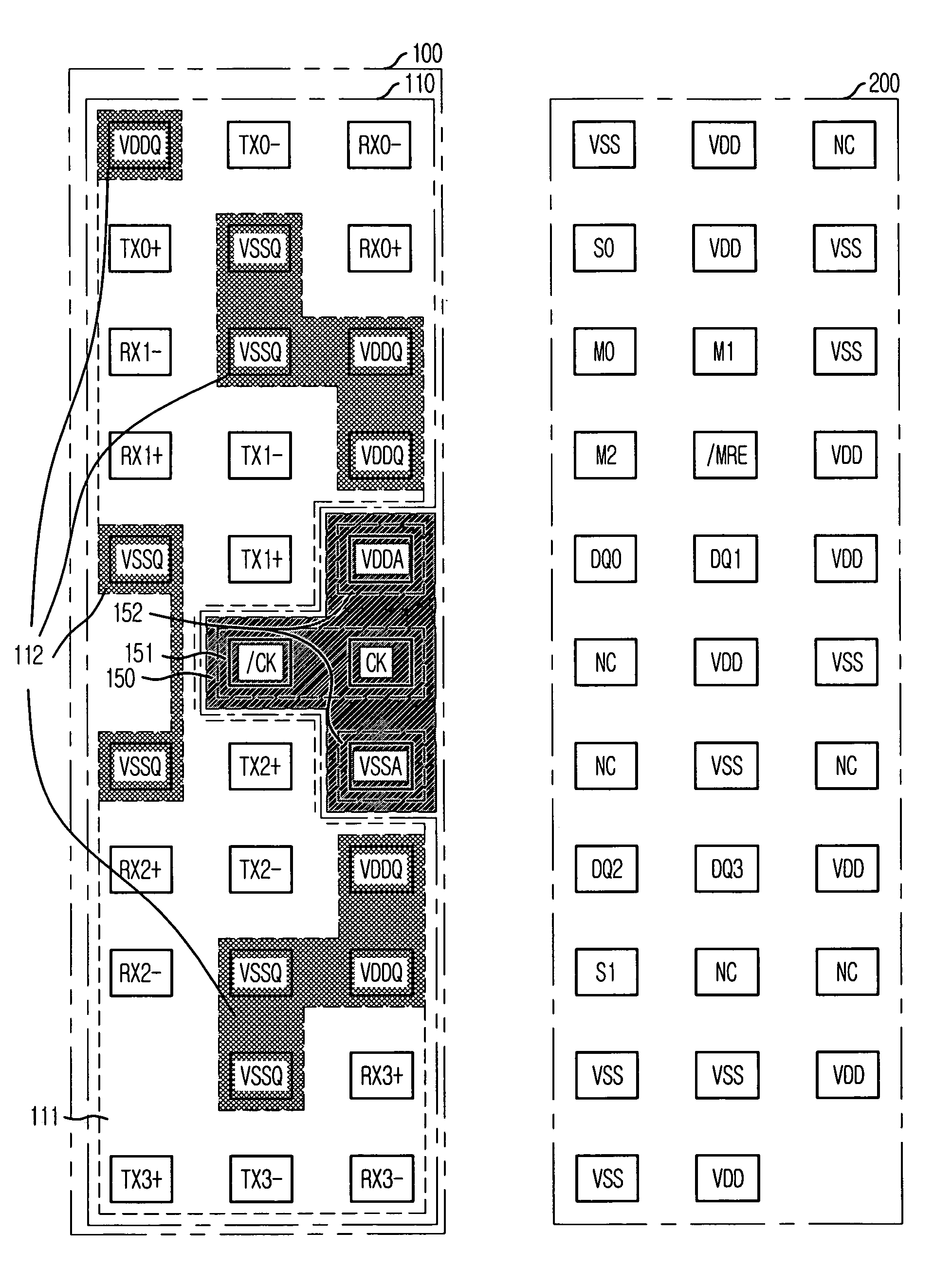
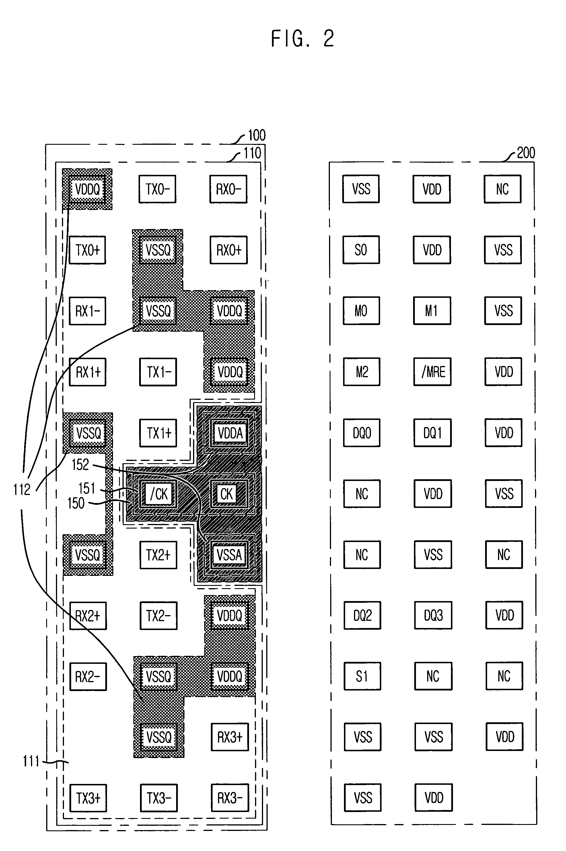
[0019]FIG. 2 is a diagram of a package ball out configuration of a multi-port memory device having a serial I / O interface in accordance with the present invention.
[0020]The package ball out configuration in accordance with the first embodiment of the present invention includes a first package ball out region 100 and a second package ball out region 200, which are arranged at the left and right sides of a vertical center line, respectively.
[0021]Balls 110 for a serial I / O interface part and balls 150 for a clock interface part are arranged in the first package ball out region 100, and balls for a DRAM interface part are arranged in the second package ball out region 200.
[0022]In the first package ball out region 100, the balls 110 for the serial I / O interface part include serial data balls 111 and serial power / ground balls 112. The serial data balls 111 are used for serial data communication TX0+ / TX0−, RX0+ / RX0−, TX1+ / TX1−, RX1+ / RX1−, TX2+ / TX2−, RX2+ / RX2−, TX3+ / TX3− and RX3+ / RX3−. Th...
second embodiment
[0026]FIG. 3 illustrates a package ball out configuration of a multi-port memory device having a serial I / O interface in accordance with the present invention.
[0027]The package ball out configuration in accordance with the second embodiment of the present invention includes a first package ball out region 300 and a second package ball out region 400, which are arranged at the left and right sides of a vertical center line, respectively.
[0028]Balls 310 for a serial I / O interface are arranged in the first package ball out region 300. Balls 450 for a clock interface part and balls 410 for a DRAM interface part are arranged in the second package ball out region 400. Since the package ball out configuration of FIG. 3 is different from that of FIG. 2 only in terms of the arrangement of the balls 450 for the clock interface part, its detailed description will be omitted for conciseness.
[0029]As described above, the power layer of the package can be easily configured by separately arranging...
PUM
 Abstract
Description
Claims
Application Information
 - R&D
- Intellectual Property
- Life Sciences
- Materials
- Tech Scout
- Unparalleled Data Quality
- Higher Quality Content
- 60% Fewer Hallucinations
Browse by: Latest US Patents, China's latest patents, Technical Efficacy Thesaurus, Application Domain, Technology Topic, Popular Technical Reports.
© 2025 PatSnap. All rights reserved.Legal|Privacy policy|Modern Slavery Act Transparency Statement|Sitemap|About US| Contact US: help@patsnap.com