
Light emitting diode with ITO layer and method for fabricating the same

a technology ito layers, which is applied in the direction of electric variable regulation, process and machine control, instruments, etc., can solve the problems of lowering the light emitting efficiency of light emitting diodes, and achieve the effect of reducing the light emitting area, improving luminance, and efficient current diffusion into the ito layer

Active Publication Date: 2010-04-20
SEOUL VIOSYS CO LTD
View PDF43 Cites 36 Cited by
  • Summary
  • Abstract
  • Description
  • Claims
  • Application Information

AI Technical Summary

Benefits of technology

[0010]Accordingly, an object of the present invention is to provide a light emitting diode with greatly enhanced luminance and light emitting performance due to the increase in efficiency of current diffusion into an ITO layer on a P-type semiconductor layer, and a method of fabricating the light emitting diode.
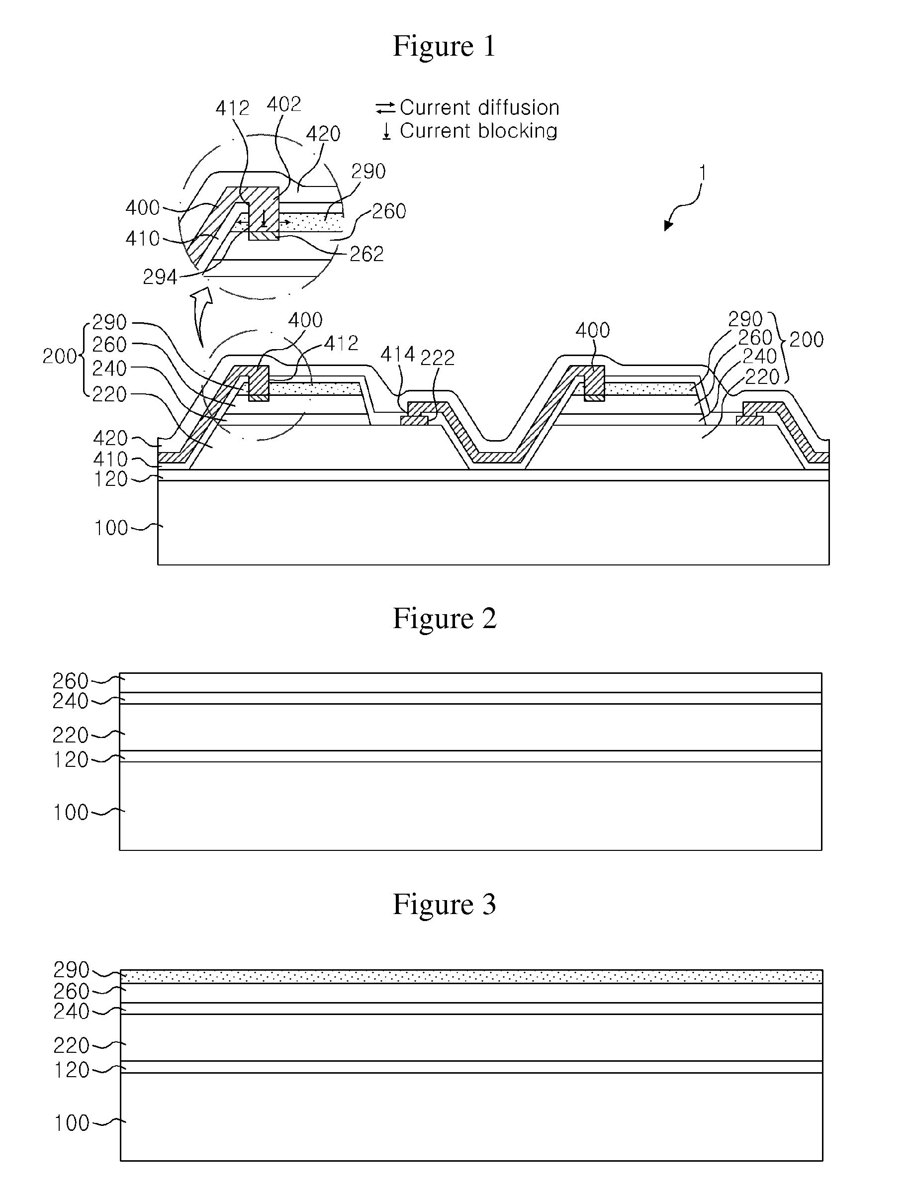
[0019]According to a structure in which a contact connection portion, i.e. an end of a wiring, or a P-type contact pad at an end of a wiring is brought into contact with an inner circumferential surface of a contact groove formed in an ITO layer, efficiency of current diffusion into an ITO layer on a P-type semiconductor layer can be enhanced without reducing a light emitting area of the ITO layer. Therefore, a light emitting diode with greatly improved luminance and light emitting performance can be implemented.
[0020]In a light emitting diode including a P-type contact pad as a contact connection portion according to an embodiment of the present invention, the P-type contact pad can simultaneously come into contact with a top surface of the ITO layer and the inner circumferential surface of the ITO layer. Consequently, a contact area between the ITO layer and the P-type contact pad is further increased such that the efficiency of current diffusion into the ITO layer can be enhanced.
[0021]For example, in a light emitting diode including a plurality of light emitting cells according to another embodiment of the present invention similar to an AC light emitting diode operated by an AC power source, a wiring may comprise a conductive material layer formed through a plating or vapor depositing process such that wiring disconnection and the like can be prevented. At this time, since the contact connection portion formed of a portion of the conductive material layer comes into contact with the inner circumferential surface of the contact groove of the ITO layer, the efficiency of current diffusion into the ITO layer can be enhanced.
[0022]Further, according to the embodiments of the present invention, a current blocking layer formed due to change in a current property of a portion of a P-type semiconductor layer during a dry etching process may be formed at a position where the P-type semiconductor layer is brought into contact with the contact connection portion. Therefore, the current blocking layer can completely block current from flowing directly into the P-type semiconductor layer to contribute in enhancing the efficiency of current diffusion into the ITO layer.

Problems solved by technology

However, since the Ni / Au layer has very low transmittance for visible light in spite of the superior electrical property, there is a problem in that the light emitting efficiency of a light emitting diode is lowered.

Method used


Image

  • Light emitting diode with ITO layer and method for fabricating the same
  • Light emitting diode with ITO layer and method for fabricating the same
  • Light emitting diode with ITO layer and method for fabricating the same

Examples


first embodiment

[0029]FIG. 1 is a sectional view showing a light emitting diode according to the present invention.

[0030]A light emitting diode 1 according to the first embodiment of the present invention is an AC light emitting diode operating under AC conditions. A conventional AC light emitting diode operated by an AC power source has been disclosed in PCT Publication No. WO 2004 / 023568 A1 entitled “Light-emitting device having light emitting element” by Sakai, et al.

[0031]Referring to FIG. 1, the light emitting diode 1 according to this embodiment comprises a substrate 100 serving as a base and a plurality of light emitting cells 200. The substrate 100 may be an insulating or conductive substrate. Although a sapphire substrate is used in this embodiment, another substrate such as SiC may be utilized.

[0032]Further, a buffer layer 120 for reducing lattice mismatch between lower layers of the light emitting cells 200 and the substrate 100 may be interposed between the substrate 100 and the light e...

second embodiment

[0058]FIG. 10 is a sectional view illustrating a light emitting diode according to the present invention.

[0059]As shown in FIG. 10, the light emitting diode 1 according to this embodiment comprises a substrate 100 serving as a base and a light emitting cell 200 formed on the substrate 100. Similarly to the previous embodiment, the light emitting cell 200 has a structure in which an N-type semiconductor layer 220, an active layer 240 and a P-type semiconductor layer 260 are sequentially laminated. The active layer 240 is restrictively formed on a certain region of the N-type semiconductor layer 220 through the aforementioned mesa formation process, and the P-type semiconductor layer 260 is formed on the active layer 240. Thus, a certain region of the N-type semiconductor layer 220 is bonded to the active layer 240, whereas the rest of the region is exposed as a contact region where an N-type contact pad 222 is formed. Further, an ITO layer 290 is formed on the P-type semiconductor la...


PUM


Abstract

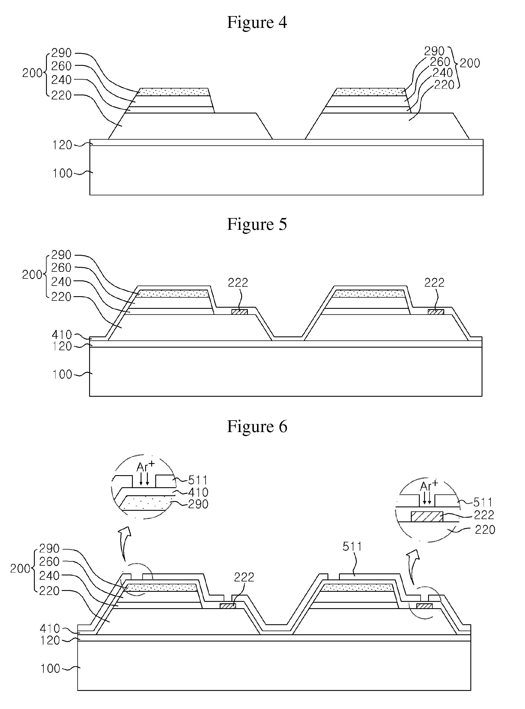
The present invention relates to a light emitting diode with enhanced luminance and light emitting performance due to increase in efficiency of current diffusion into an ITO layer, and a method of fabricating the light emitting diode. According to the present invention, there is manufactured at least one light emitting cell including an N-type semiconductor layer, an active layer and a P-type semiconductor layer on a substrate. The method of the present invention comprises the steps of (a) forming at least one light emitting cell with an ITO layer formed on a top surface of the P-type semiconductor layer; (b) forming a contact groove for wiring connection in the ITO layer through dry etching; and (c) filling the contact groove with a contact connection portion made of a conductive material for the wiring connection.

Description

CROSS REFERENCE RELATED APPLICATIONS[0001]This application is a continuation application of U.S. patent application Ser. No. 12 / 088,902, filed on Apr. 1, 2008, which is the National Stage of International Application No. PCT / KR2006 / 005352, filed Dec. 8, 2006, and claims priority from and the benefit of Korean Patent Application No. 10-2006-0002421, filed on Jan. 9, 2006, and Korean Patent Application No. 10-2006-0023612, filed Mar. 14, 2006, which are all hereby incorporated by reference for all purposes as if fully set forth herein.BACKGROUND OF THE INVENTION[0002]1. Field of the Invention[0003]The present invention relates to a light emitting diode with a transparent ITO layer as an electrode layer and a method of fabricating the light emitting diode, and more particularly, to a light emitting diode with enhanced luminance and light emitting performance due to increase in efficiency of current diffusion into an ITO layer, and a method of fabricating the light emitting diode.[0004]...

Claims


Application Information

Patent Timeline
Patent Type & Authority Patents(United States)
IPC IPC(8): H01L33/00H01L27/15H01L33/06H01L33/08H01L33/32H01L33/42
CPCH01L33/42H01L33/62H01L27/153H01L2924/0002H01L2924/00
Inventor KIM, DAE WONYOON, YEO JINOH, DUCK HWANKIM, JONG HWAN
Owner SEOUL VIOSYS CO LTD
Learn More