Circuit board connector

a technology for connecting components and circuit boards, applied in the direction of securing/insulating coupling contact members, coupling device connections, fixed connections, etc., can solve the problems of inducing cracks in the portions of the board, undetectable stress, etc., and achieve the effect of facilitating deformation and absorbing stress

Inactive Publication Date: 2010-04-27
YAZAKI CORP
View PDF10 Cites 56 Cited by
  • Summary
  • Abstract
  • Description
  • Claims
  • Application Information

AI Technical Summary

Benefits of technology

[0009]In view of the above-described circumstances, an object of the invention is to provide a circuit board connector which, even in a case where a thermal contraction difference occurs between the circuit board and the connector housing owing to a thermal cycle or the like, is capable of alleviating stresses occurring in the terminals and of ensuring that cracks are not be formed in the portions of the terminals which are soldered to the circuit board.
[0014]According to the above-described first aspect of the invention, the stress absorbing portion is provided in the rear of the press-fitting portion of the terminal, i.e., midway in the coupling portion coupling the press-fitting portion with the board fixing portion. Therefore, even in a case where a stress has occurred between the press-fitting portion and the board fixing portion owing to such as a thermal contraction difference between the connector housing and the circuit board, it is possible to absorb the stress as the stress absorbing portion is deformed. Accordingly, an undue stress ceases to be applied to a portion of the board fixing portion which is soldered to the circuit board, and it is thereby possible to prevent in advance a crack from being formed in the soldered portion and enhance the connection reliability of the soldered portion.
[0017]According to the above-described fourth aspect of the invention, since the inner or outer width between the second opposing two sides of the stress absorbing portion is made greater than a width of the first straight portion, the opposing two sides in the left-right direction can be easily deformed to absorb the stress.

Problems solved by technology

With this type of circuit board connector, there has been a problem in that since the terminals 110A and 110B are press-fitted into and fixed in the connector housing 101, in a case where a thermal contraction difference has occurred between the circuit board and the connector housing owing to a thermal cycle or the like, stresses are undesirably generated in the terminals 110A and 110B, possibly inducing cracks in the portions of the board fixing portions 117 which are soldered to the circuit board.

Method used


Image

  • Circuit board connector
  • Circuit board connector
  • Circuit board connector

Examples


Embodiment Construction

[0027]Referring now to the accompanying drawings, a description will be given of an embodiment of the invention.

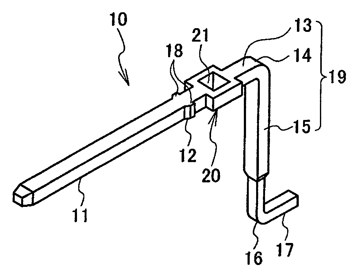
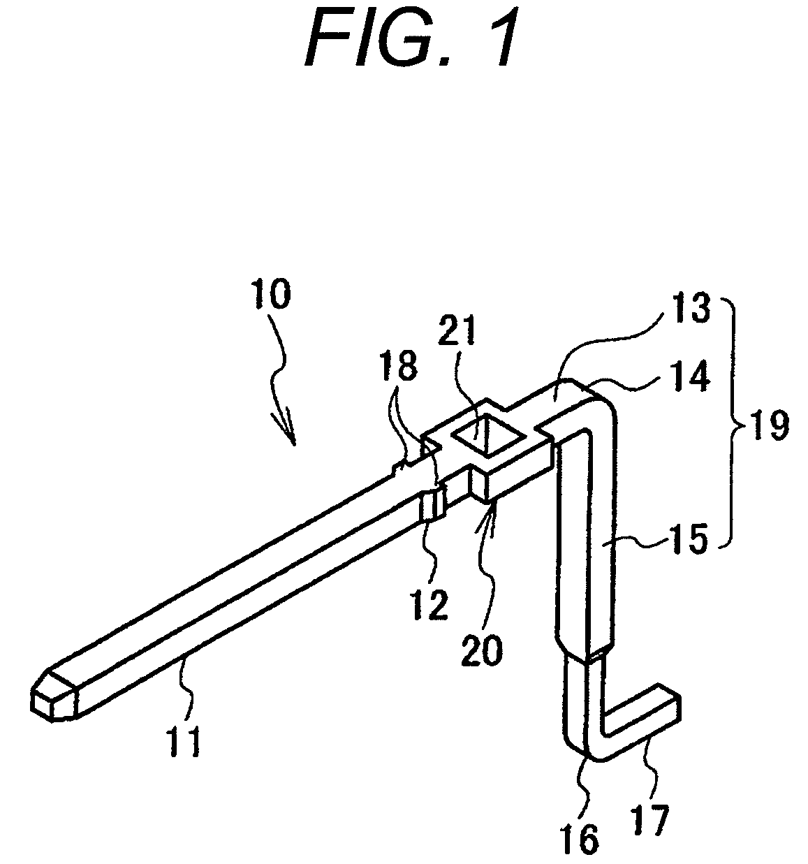
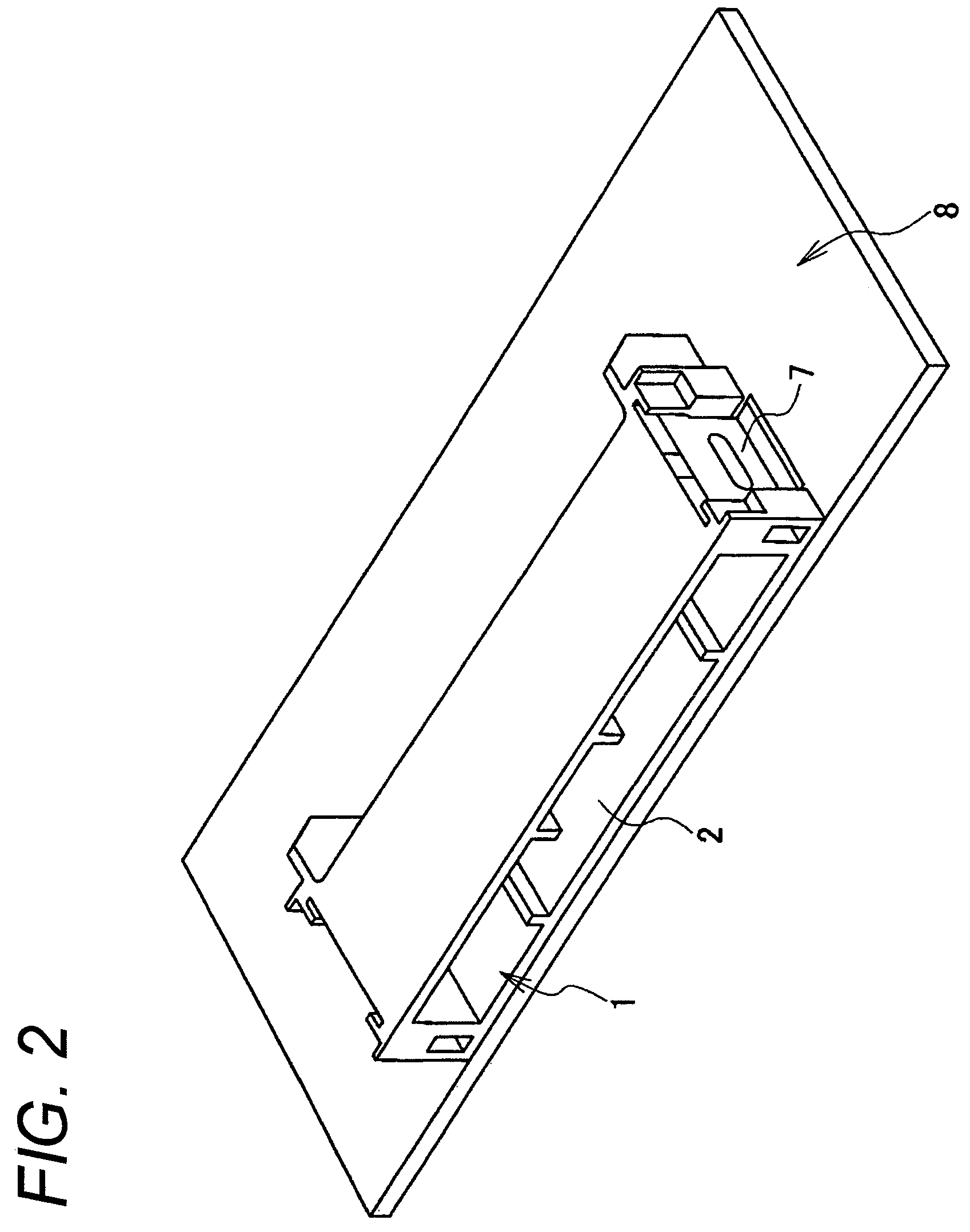
[0028]FIG. 1 is a perspective view illustrating the construction of a terminal which is used in the circuit board connector in accordance with the embodiment. FIG. 2 is an external perspective view taken from the front side of the circuit board connector in accordance with the embodiment. FIG. 3 is an external perspective view taken from the rear side of that circuit board connector. FIG. 4 is a rear view of essential portions of the circuit board connector. FIG. 5 is a partial enlarged view thereof. FIG. 6 is a horizontal cross-sectional view of that circuit board connector. FIG. 7 is a partial enlarged view thereof.

[0029]As shown in FIGS. 1 to 7, the circuit board connector in accordance with this embodiment is comprised of a resin-made connector housing 1 which is mounted on a circuit board 8 such that the front-back direction of the circuit board connector is oriented ...


PUM


Abstract

A circuit board connector is provided. The circuit board connector includes: a connector housing which is mounted on a circuit board; and a terminal which is press-fitted into the terminal press-fitting hole of the connector housing. The terminal includes: a terminal connecting portion which is disposed through the rear side of the connector housing to be connected to a mating connector; a press-fitting portion to be fixed to the connector housing; a board fixing portion fixed to the circuit board by soldering; and a coupling portion extending and bent toward a side of the circuit board to couple the press-fitting portion with the board fixing portion. The circuit board connector also includes a stress absorbing portion provided with a center hole which is provided on a midway of the coupling portion so as to absorb a stress by being deformed.

Description

BACKGROUND OF THE INVENTION[0001]1. Technical Field[0002]The present invention relates to a circuit board connector which is mounted on a circuit board.[0003]2. Background Art[0004]Examples of this type of circuit board connector are shown in, for example, JP-A-2006-100231 and JP-A-2005-116230. FIG. 8 is a schematic diagram of a circuit board connector described in JP-A-2006-100231. FIGS. 9A and 9B are schematic diagrams of terminals of the connector.[0005]As shown in FIG. 8, the circuit board connector is comprised of a resin-made connector housing 101 having in its front portion a fitting port 102 for fitting to a mating connector, as well as a multiplicity of metallic terminals 110A and 110B which are press-fitted from the rear side into terminal press-fitting holes 104 in a rear wall 103 of the connector housing 101 and are fixed therein.[0006]Of the two kinds of terminals 110A and 110B, the terminal 110A shown in FIG. 9A is press-fitted into the terminal press-fitting hole 104 ...

Claims


Application Information

Patent Timeline
Patent Type & Authority Patents(United States)
IPC IPC(8): H01R13/64
CPCH01R12/57H01R12/707H01R13/40H01R12/714H01R12/716H01R12/724
Inventor SAKAMOTO, NOBUYUKI
Owner YAZAKI CORP
Why Eureka
Try Eureka