Substrate for growing a III-V light emitting device

a technology of iii-v light emitting devices and substrates, which is applied in the direction of crystal growth process, polycrystalline material growth, electrolytic capacitors, etc., can solve the problems of poor performance and reliability, non-iii-nitride substrates are less than optimal, and the substrates are generally expensive and not widely available. to achieve the effect of reducing the strain in the semiconductor structur

Active Publication Date: 2007-03-29
LUMILEDS
View PDF20 Cites 250 Cited by
  • Summary
  • Abstract
  • Description
  • Claims
  • Application Information

AI Technical Summary

Benefits of technology

[0008] In accordance with embodiments of the invention, a substrate including a host and a seed layer bonded to the host is provided, then a semiconductor structure including a light emitting layer disposed between an n-type region and a p-type region is grown on the seed layer. In some embodiments, a bonding layer bonds the host to the seed layer. In some embodiments, the seed layer may be thinner than a critical thickness for relaxation of strain in the semiconductor structure, such that strain in the semiconductor structure is relieved by dislocations formed in the seed layer, or by gliding between the seed layer and bonding layer at the interface between these layers. In some embodiments, the difference between the lattice constant of the seed layer and the lattice constant of a nucleation layer in the semiconductor structure is less than 1%. In some embodiments, the coefficient of thermal expansion of the host is at least 90% of the coefficient of thermal expansion of at least one layer of the semiconductor structure. In some embodiments, trenches are formed in the seed layer to reduce strain in the semiconductor structure. In some embodiments, the host may be separated from the semiconductor structure and seed layer by etching away the bonding layer with an etch that preferentially attacks the bonding layer over the semiconductor structure.

Problems solved by technology

Since native III-nitride substrates are generally expensive and not widely available, III-nitride devices are often grown on sapphire or SiC substrates.
Such non-III-nitride substrates are less than optimal for several reasons.
First, sapphire and SiC have different lattice constants than the III-nitride layers grown on them, causing strain and crystal defects in the III-nitride device layers, which can cause poor performance and reliability problems.
Laser dissociation generates shocks waves in the semiconductor layers which can damage the semiconductor or contact layers, potentially degrading the performance of the device.

Method used


Image

  • Substrate for growing a III-V light emitting device
  • Substrate for growing a III-V light emitting device
  • Substrate for growing a III-V light emitting device

Examples


Embodiment Construction

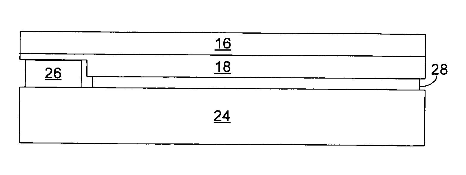
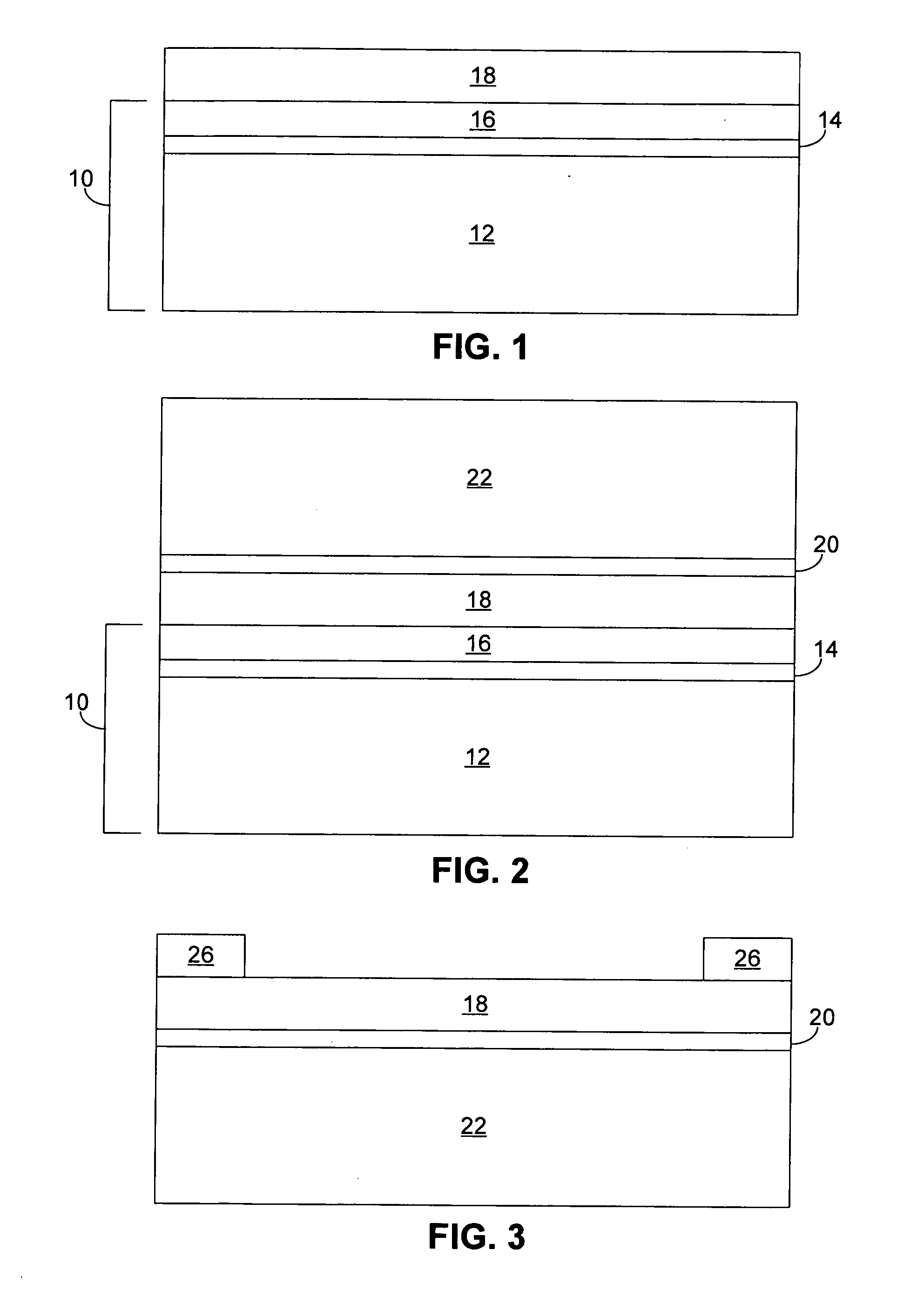
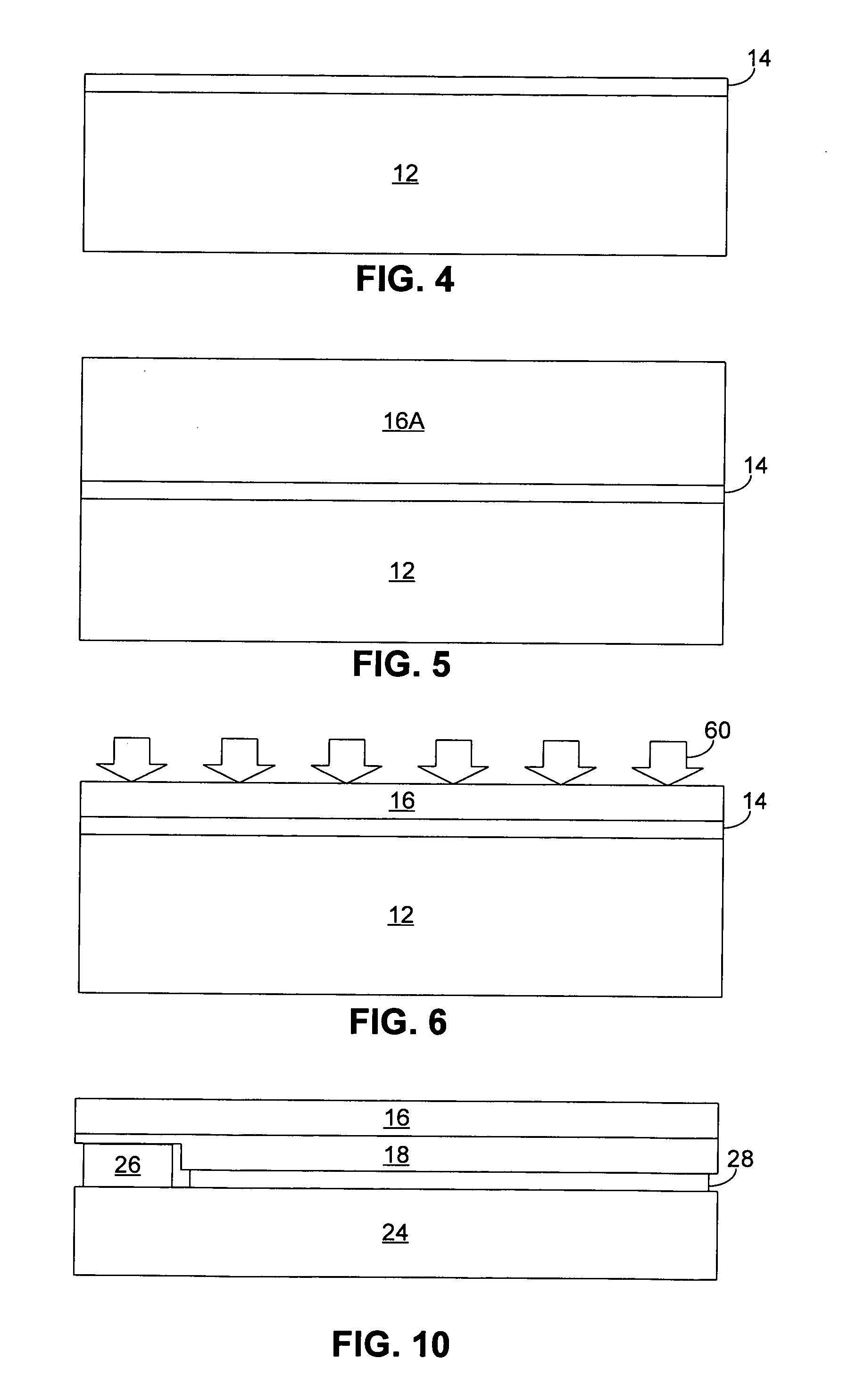
[0019] In accordance with embodiments of the invention, a semiconductor light emitting device such as a III-nitride light emitting device is grown on a composite growth substrate 10, as illustrated in FIG. 1. Substrate 10 includes a host substrate 12, a seed layer 16, and a bonding layer 14 that bonds host 12 to seed 16. Each of the layers in substrate 10 are formed from materials that can withstand the processing conditions required to grow the semiconductor layers in the device. For example, in the case of a III-nitride device grown by MOCVD, each of the layers in substrate 10 must be able to tolerate an H2 ambient at temperatures in excess of 1000° C.; in the case of a III-nitride device grown by MBE, each of the layers in substrate 10 must be able to tolerate temperatures in excess of 600° C. in a vacuum.

[0020] Host substrate 12 provides mechanical support to substrate 10 and to the semiconductor device layers 18 grown over substrate 10. Host substrate 12 is generally between 3...


PUM


Abstract

A substrate including a host and a seed layer bonded to the host is provided, then a semiconductor structure including a light emitting layer disposed between an n-type region and a p-type region is grown on the seed layer. In some embodiments, a bonding layer bonds the host to the seed layer. The seed layer may be thinner than a critical thickness for relaxation of strain in the semiconductor structure, such that strain in the semiconductor structure is relieved by dislocations formed in the seed layer, or by gliding between the seed layer and the bonding layer an interface between the two layers. In some embodiments, the host may be separated from the semiconductor structure and seed layer by etching away the bonding layer.

Description

BACKGROUND [0001] 1. Field of Invention [0002] This invention relates to semiconductor light emitting devices such as light emitting diodes and, in particular, to growth substrates on which such light emitting devices may be grown. [0003] 2. Description of Related Art [0004] Semiconductor light-emitting devices including light emitting diodes (LEDs), resonant cavity light emitting diodes (RCLEDs), vertical cavity laser diodes (VCSELs), and edge emitting lasers are among the most efficient light sources currently available. Materials systems currently of interest in the manufacture of high-brightness light emitting devices capable of operation across the visible spectrum include Group III-V semiconductors, particularly binary, ternary, and quaternary alloys of gallium, aluminum, indium, and nitrogen, also referred to as III-nitride materials. Typically, III-nitride light emitting devices are fabricated by epitaxially growing a stack of semiconductor layers of different compositions a...

Claims


Application Information

Patent Timeline
Patent Type & Authority Applications(United States)
IPC IPC(8): H01L21/00H01G9/20H01L33/00
CPCC30B25/183C30B29/40C30B29/403H01L33/0079H01L21/76256H01L33/007H01L21/76254H01L33/0093
Inventor KRAMES, MICHAEL R.GARDNER, NATHAN F.EPLER, JOHN E.
Owner LUMILEDS
Why Eureka
Try Eureka