Simulator and parameter extraction device for transistor, simulation and parameter extraction method for transistor, and associated computer program and storage medium

a transistor and simulation device technology, applied in the field of transistor simulators, can solve the problems of difficult parameter extraction, complex alternative equations, and inability to readily carry out accurate characteristics simulation of transistors, and achieve good fit with capacitance models, high accuracy, and high accuracy

Inactive Publication Date: 2010-05-04
SHARP KK +1
View PDF15 Cites 4 Cited by
  • Summary
  • Abstract
  • Description
  • Claims
  • Application Information

AI Technical Summary

Benefits of technology

[0020]As a result, despite the fact that the transistor including regions of mutually different impurity concentrations below the gate section is the simulation target, the characteristics of a transistor, inclusive of subthreshold regions which are difficult to evaluate through actual measurement, can be simulated to high accuracy while preserving a good fit with a capacitance model. In addition, the characteristics of the transistor are simulated using a model equation including threshold parameters which has physical meanings; therefore, parameters can highly accurately be extracted from the measurements of the characteristics of the simulation target transistor.
[0028]According to the arrangement, when regarding the channel region as a primary factor of resistance variations between the source section electrode and the drain section electrode of the transistor and the other regions providing parasitic resistance, the terms corresponding respectively to the primary factor region and the parasitic resistance regions include threshold parameters which are set independently from each other. Therefore, by the simulation of a transistor with the model equation, despite the fact that the transistor including regions of mutually different impurity concentrations below the gate section is the simulation target, the characteristics of a transistor, inclusive of subthreshold regions which are difficult to evaluate through actual measurement, can be simulated to high accuracy while preserving a good fit with a capacitance model.
[0029]In addition, the parameter extraction device extracts threshold parameters on the basis of the characteristics of the capacitance of a transistor with respect to the gate voltage; therefore, a single measurement of the characteristics of the capacitance with respect to the gate voltage can extract all the threshold parameters, regardless of the number of threshold parameters. Therefore, the threshold parameters included in the model equation which can simulate the characteristics of a transistor to high accuracy can readily be extracted.
[0035]According to the arrangement, when regarding the channel region as a primary factor of resistance variations between the source section electrode and the drain section electrode of the transistor and the other regions providing parasitic resistance, the terms corresponding respectively to the primary factor region and the parasitic resistance regions include threshold parameters which are set independently from each other. Therefore, despite the fact that the transistor including regions of mutually different impurity concentrations below the gate section is the simulation target, the characteristics of a transistor, inclusive of subthreshold regions which are difficult to evaluate through actual measurement, can be simulated to high accuracy while preserving a good fit with a capacitance model.
[0043]According to the arrangement, the threshold parameters are extracted on the basis of the characteristics of the capacitance of a transistor with respect to the gate voltage; therefore, a single measurement of the characteristics of the capacitance with respect to the gate voltage can extract all the threshold parameters, regardless of the number of threshold parameters. Therefore, the threshold parameters included in the model equation which can simulate the characteristics of a transistor to high accuracy can readily be extracted.

Problems solved by technology

However, with the equation, one cannot readily carry out a accurate characteristics simulation for a transistor (second transistor) in which there exist multiple impurity concentration regions below the gate section.
This alternative equation however is more complicated.
In addition, with alternative model equations simulating a different moving carrier mobility μ from the first transistor, parameter extraction is difficult and simulatable gate length ranges are narrower, because the model equations disregards the physical fact that the first and second transistors have the same moving carrier mobility, except in the impurity concentration regions found in the second transistor, but not in the first transistor.
Thus, the approach poorly matches capacitance models based on the behavior of surface charge in the channel section and renders it difficult to improve the fitting accuracy of simulation where evaluation through actual measurement is difficult, as in subthreshold regions.

Method used


Image

  • Simulator and parameter extraction device for transistor, simulation and parameter extraction method for transistor, and associated computer program and storage medium
  • Simulator and parameter extraction device for transistor, simulation and parameter extraction method for transistor, and associated computer program and storage medium
  • Simulator and parameter extraction device for transistor, simulation and parameter extraction method for transistor, and associated computer program and storage medium

Examples


embodiment 1

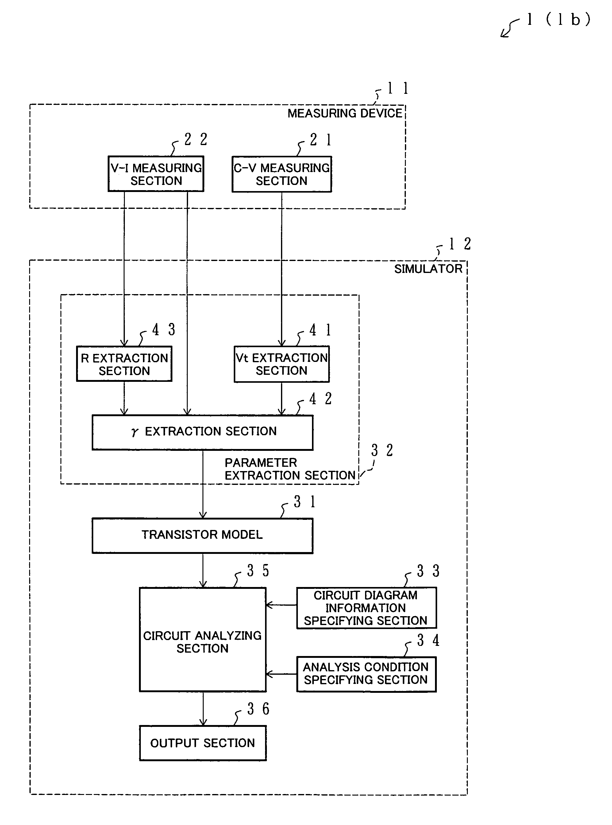
[0070]The following will describe an embodiment of the present invention with reference to FIGS. 1 through 20. A simulation system (simulator) 1 in accordance with the present embodiment is capable of simulate the characteristics of a field effect transistor 2 to high accuracy. The transistor 2 includes regions of different resistance values below its gate section.

[0071]The field effect transistor 2 which is a simulation target for the simulation system 1 (“transistor 2”) may be of any structure as long as it has regions of different resistance values below its gate section. The following description will assume, as an example, that the transistor 2 be a thin film transistor fabricated on glass or another insulating substrate.

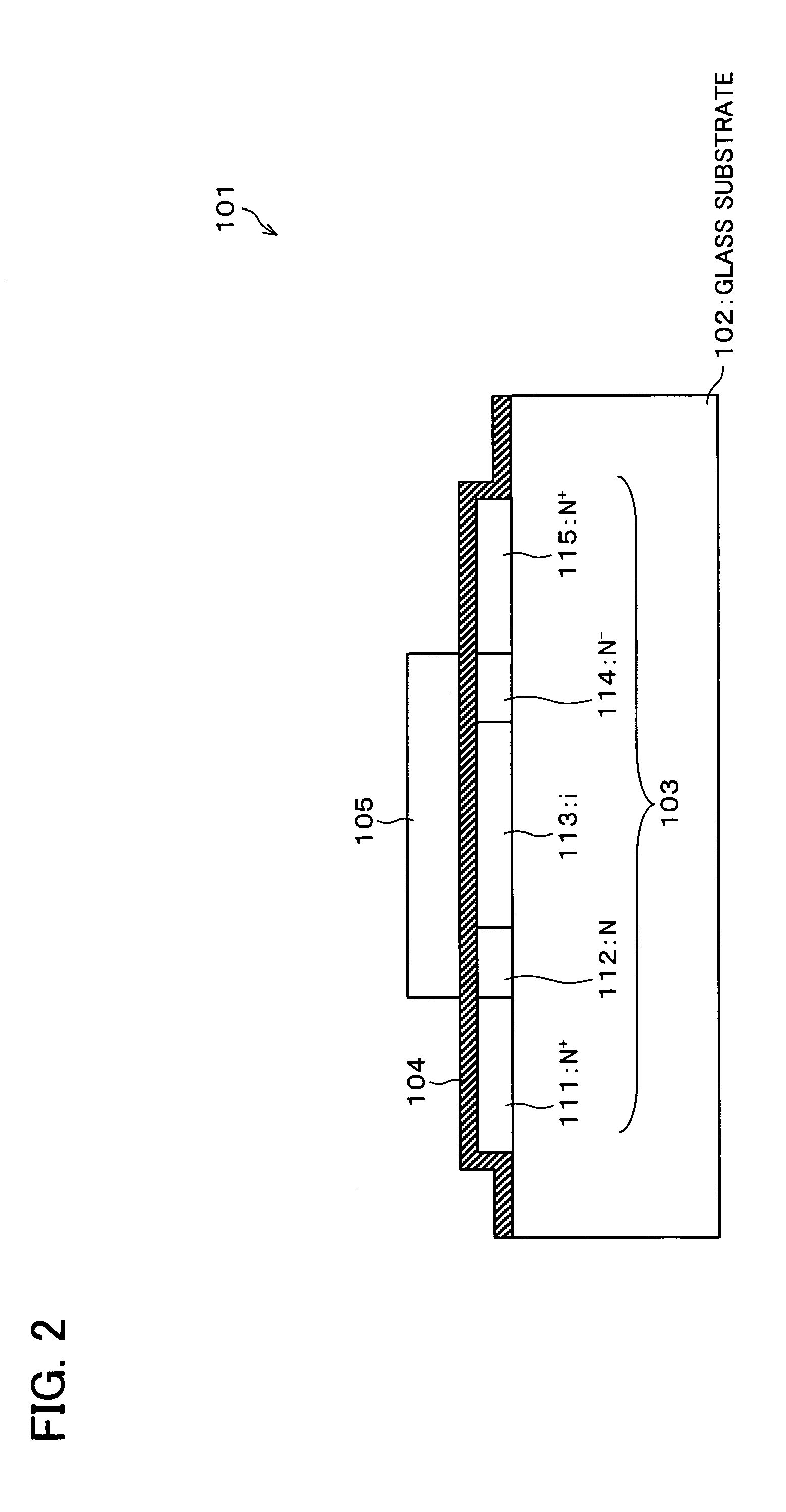
[0072]A thin film transistor 101 includes a thin film (e.g. polycrystalline silicon thin film) formed on an insulating substrate as an active layer, and includes a semiconductor thin film 103 on an insulating substrate 102 with a silicon oxide film (not shown) ...

embodiment 2

[0146]So far, the description discussed examples involving three regions of different impurity concentrations below a gate section as shown, for example, in FIG. 2. The number of such regions is not limited to this. For example, four or more regions may be provided as shown in FIG. 21 and FIG. 23.

[0147]The present embodiment will deal with more general cases, assuming that n regions of different impurity concentrations (n is an integer more than or equal to 2) are provided below a gate section. In other words, it is assumed that adjacent areas A1 to An of different impurity concentrations were provided below a gate section.

[0148]On that assumption, the simulation system 1 in accordance with the present embodiment uses equations (10), (11) below instead of equations (5), (6) above in modeling:

[0149]Rds=Vd / Id=∑[Li / {(Wi·μi·Coxi)·(Vg-Vti)}]+R(10)⁢=∑[γi / (Vg-Vti)]+R(11)

where Σ is a summation symbol with the index i from 1 to n.

[0150]For example, an FET 101c shown in FIG. 21 has a substant...

embodiment 3

[0182]The present embodiment will describe a simulation system 1b capable of simulating the characteristics of a simulation target transistor 2 to higher accuracy than the first and second embodiments if the transistor 2 is symmetric with respect to the center line of an area functioning as a channel region.

[0183]The simulation system 1b in accordance with the present embodiment has a substantially similar structure as the simulation system 1 in FIG. 1. A transistor model 31 however models the transistor 2 with equation (16) instead of equations (5) through (8) and equations (10) through (13):

Rds=Vd / Id=Σ[γi / (Vg−Vti)]+γn / (Vg−Vtn−Vd / 2)+R  (16)

where the number of regions is taken as 2n−1, and Σ is a summation symbol with the index i from 1 to 2n−1, except for i=n.

[0184]In equation (16), only the term corresponding to an area which is functioning as the channel region and which is an impurity concentration region which is a primary factor of resistance variations between the source sect...


PUM


Abstract

A transistor model for a simulator simulates a resistance between a source region and a drain region with a model equation which has terms representing resistance values corresponding respectively to areas of mutually different impurity concentrations below a gate section in simulating characteristics of a transistor. At least two of the terms each having a threshold parameter indicating a voltage at which a semiconductor element composed of the associated region and regions adjacent to that region changes from an ON state to an OFF state. The threshold parameters of the terms being specified independently from each other. Thus, the characteristics of a transistor having a set of areas of mutually different impurity concentrations below a gate section, inclusive of subthreshold regions which are difficult to evaluate through actual measurement, can be simulated to high accuracy while preserving a good fit with a capacitance model.

Description

[0001]This Nonprovisional application claims priority under 35 U.S.C. §119(a) on Patent Application No. 2003 / 197902 filed in Japan on Jul. 16, 2003, the entire contents of which are hereby incorporated by reference.FIELD OF THE INVENTION[0002]The present invention relates to a transistor simulator, a transistor parameter extraction device, a transistor simulation method, a transistor parameter extraction method, and an associated computer program and a storage medium.BACKGROUND OF THE INVENTION[0003]Simulators have been in widespread use which simulate the characteristics of transistors by evaluating model equations, many of which assume that there extend a single resistance region below the gate section of the transistor.[0004]An example of such a model equation is:Vd / Id=Leff / [Weff·μ·Cox·(Vg−Vt−Vd / 2)]+R  (1)where Vd is the source-to-drain voltage, Id the source-to-drain current, Vg the gate-to-source voltage, R the resistance value of a part of source and drain regions which are no...

Claims


Application Information

Patent Timeline
Patent Type & Authority Patents(United States)
IPC IPC(8): G06F7/60G06G7/62G06F17/50H01L21/336H01L29/00H01L29/78H01L29/786
CPCG06F17/5036G06F30/367
Inventor MAEDA, KAZUHIROSAKAI, TAMOTSUKUBOTA, YASUSHIIMAI, SHIGEKITADA, KENSHITANIGUCHI, KENJI
Owner SHARP KK
Why Eureka
Try Eureka