CMOS image sensor having wide dynamic range
a dynamic range, image sensor technology, applied in the direction of instruments, television systems, television system scanning details, etc., can solve the problems of affecting the image quality
- Summary
- Abstract
- Description
- Claims
- Application Information
AI Technical Summary
Benefits of technology
Problems solved by technology
Method used
Image

Examples
first embodiment
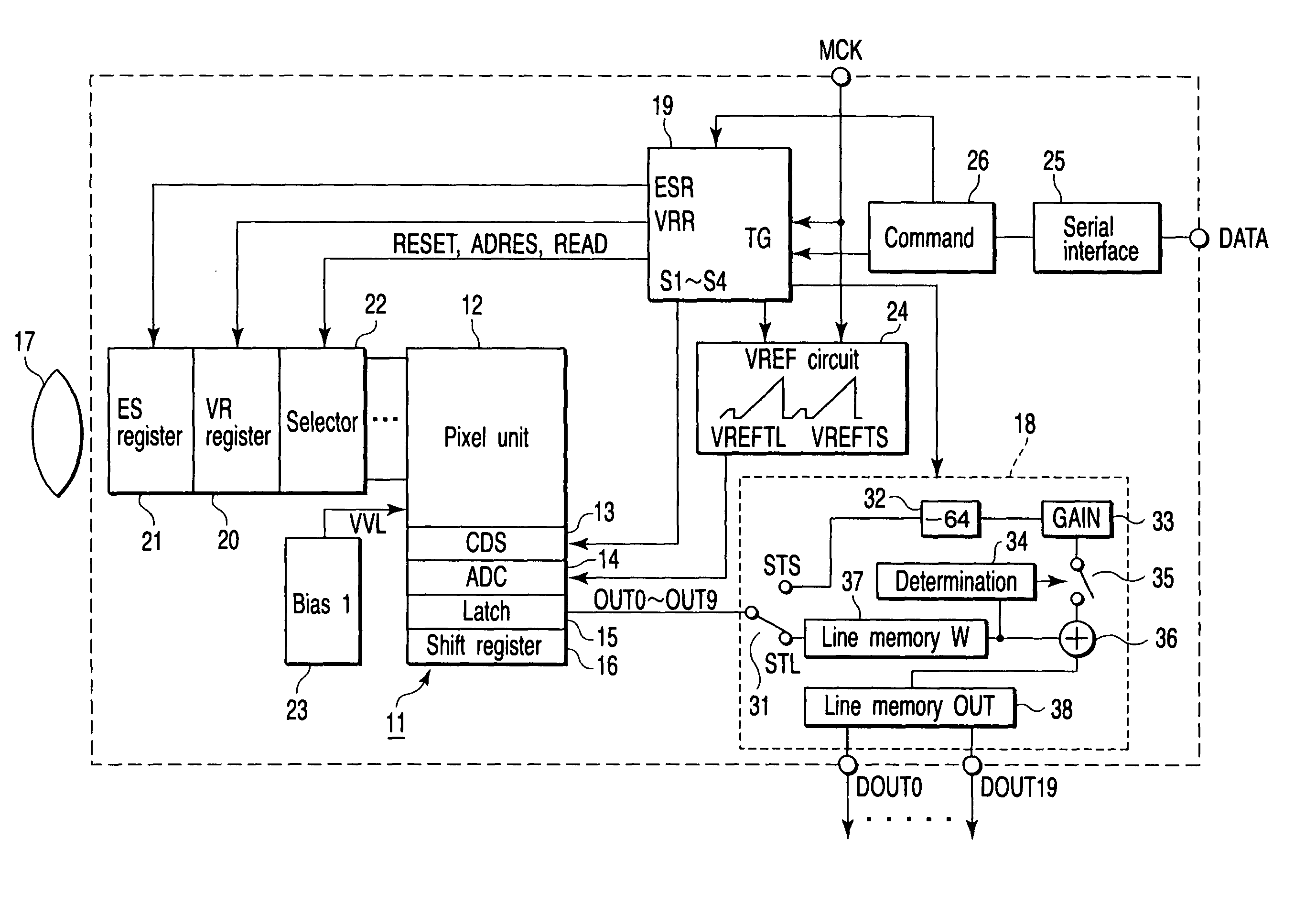
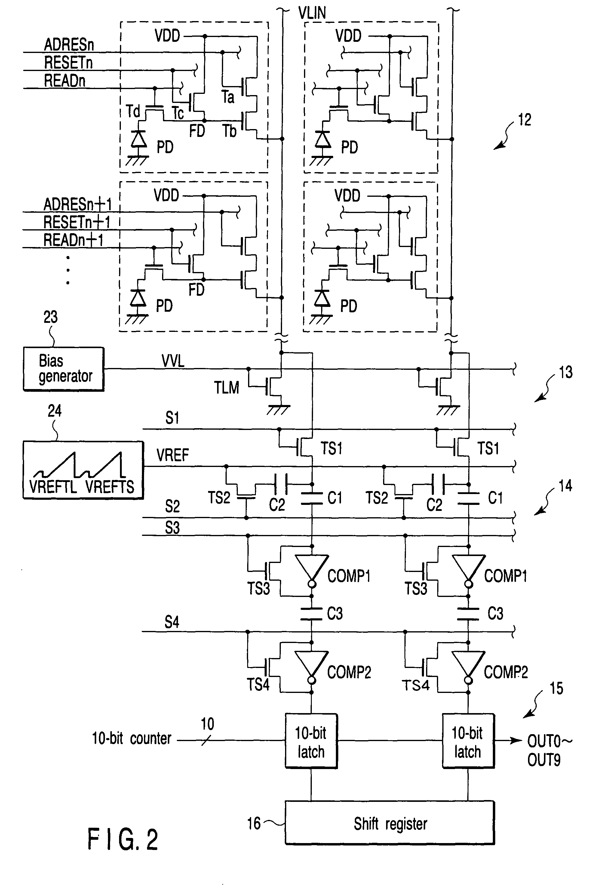
[0038]FIG. 1 is a block diagram for explaining a solid-state image sensing device according to the first embodiment of the present invention, in which an outline of the arrangement of an amplification type CMOS image sensor is illustrated. A sensor core 11 includes a pixel unit (or a pixel section) 12, column type noise canceller (CDS) 13, column type analog-to-digital converter (ADC) 14, latch circuit 15, and horizontal shift register 16. Light enters the pixel unit 12 through a lens 17, and an electric charge corresponding to the incident light amount is generated by photoelectric conversion. An analog signal corresponding to the generated electric charge is supplied to the ADC 14 via the CDS 13 and converted into a digital signal, and this digital signal is latched by the latch circuit 15. The digital signal latched by the latch circuit 15 is sequentially transferred to the shift register 16 and read out. Digital signals OUT0 to OUT9 read out from the shift register 16 are suppli...
second embodiment
[0056]As a solid-state image sensing device according to the second embodiment of the present invention, an example in which the storage time TS in the timing chart shown in FIG. 3 is 1 H or more will be explained below.
[0057]FIG. 4 is a block diagram for explaining the solid-state image sensing device according to the second embodiment of the present invention, in which an outline of the arrangement of an amplification type CMOS image sensor is illustrated. This circuit shown in FIG. 4 differs from that shown in FIG. 1 in that a vertical register (WD register, a register for controlling a short storage time) 27 for data read from a pixel unit 12 is formed. In addition, a WDM circuit 18 has five line memories W (line memories W1 to W5: 37-1 to 37-5). The output signal of this sensor has 17 bits (DOUT0 to DOUT16).
[0058]The rest of the basic configuration is the same as the circuit shown in FIG. 1, so the same reference numerals denote the same parts, and a detailed explanation thereo...
third embodiment
[0064]As a solid-state image sensing device according to the third embodiment of the present invention, an example in which the storage time TS is set at 1 H or more without increasing the number of line memories will be explained below.
[0065]FIG. 6 is a block diagram for explaining the solid-state image sensing device according to the third embodiment of the present invention, in which an outline of the arrangement of an amplification type CMOS image sensor is illustrated. The circuit shown in FIG. 6 differs from that shown in FIG. 4 in that a pulse amplitude controller 28 for controlling the amplitude of a pixel driving pulse is applied to a pulse signal VREAD. Also, when a signal STL is input to a WDM circuit 18, output signals OUT0 to OUT9 of a latch circuit 15 are input to an adder 36. When a signal STS is input, this signal is input to a line memory W 37 after −64 LSB processing. The output signal from the line memory W 37 is input to a gain circuit 33 and determination circui...
PUM
 Abstract
Description
Claims
Application Information
 - R&D
- Intellectual Property
- Life Sciences
- Materials
- Tech Scout
- Unparalleled Data Quality
- Higher Quality Content
- 60% Fewer Hallucinations
Browse by: Latest US Patents, China's latest patents, Technical Efficacy Thesaurus, Application Domain, Technology Topic, Popular Technical Reports.
© 2025 PatSnap. All rights reserved.Legal|Privacy policy|Modern Slavery Act Transparency Statement|Sitemap|About US| Contact US: help@patsnap.com