Method and apparatus for self gate pumped NMOS high speed switch

a high-speed switch, self-pumping technology, applied in mechanical equipment, machines/engines, pulse techniques, etc., can solve problems such as low resistance, use of pmos-nmos switches, and low resistan

Active Publication Date: 2010-06-22
INTEGRATED DEVICE TECH INC
View PDF3 Cites 0 Cited by
  • Summary
  • Abstract
  • Description
  • Claims
  • Application Information

AI Technical Summary

Benefits of technology

[0032]a first inverter having an input and an output; said input capable of being operative

Problems solved by technology

Problems arise when one tries to use PMOS-NMOS switches at high frequencies (e.g. above 100 MHz).
Due to the significant parasitic junction and gate oxide capacitance, it has been a challenge to build a low ON resistance switch opera

Method used


Image

  • Method and apparatus for self gate pumped NMOS high speed switch
  • Method and apparatus for self gate pumped NMOS high speed switch
  • Method and apparatus for self gate pumped NMOS high speed switch

Examples


Embodiment Construction

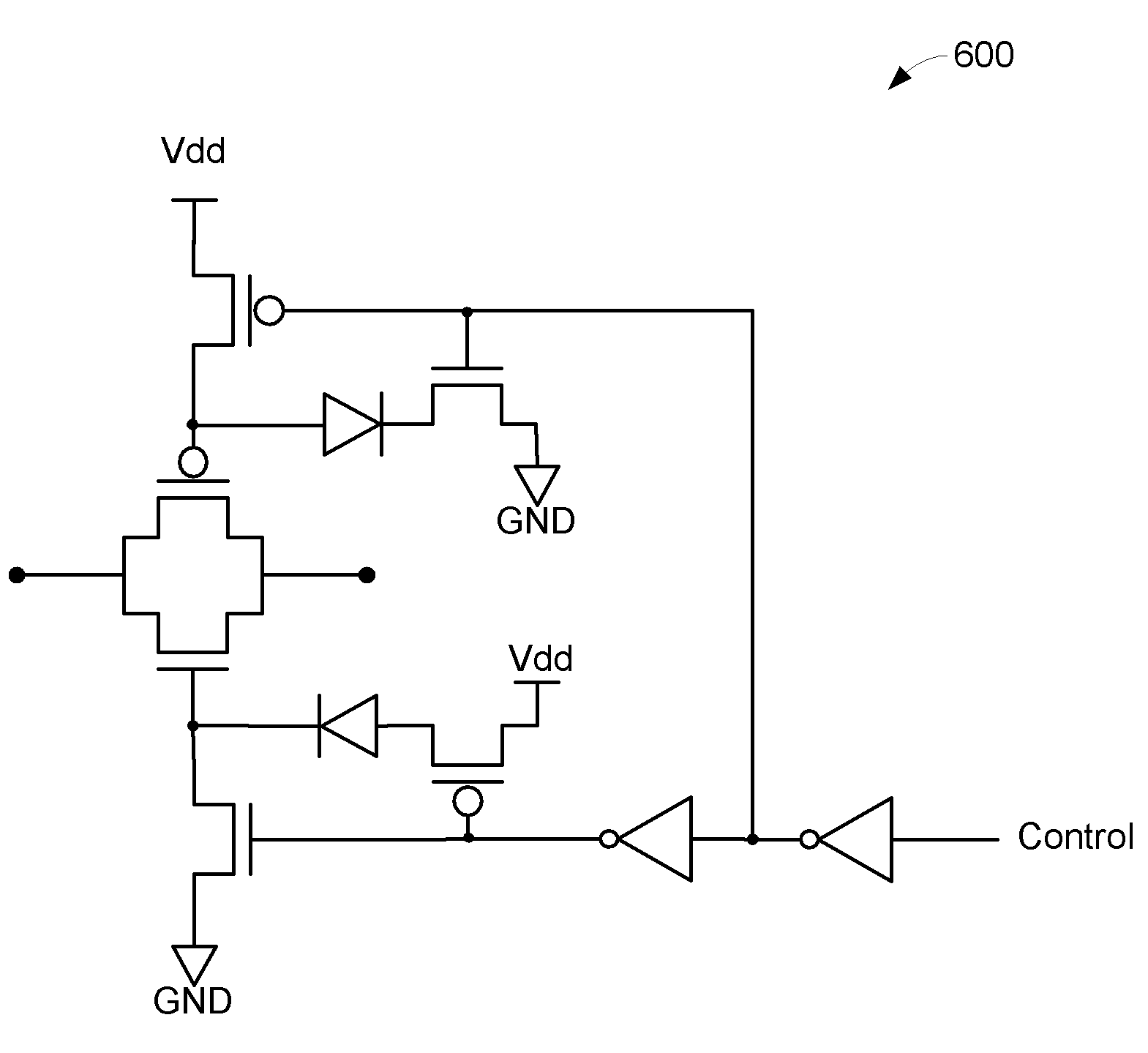
[0038]In one embodiment of the invention, an NMOS transistor with a diode and a series transistor from a supply voltage source is tied to the NMOS transistor's gate. To turn the switch off, another transistor between the gate and the ground is used. Controlling the gate voltage of this drive transistor will either short the switch transistor's gate to the ground or let it be pulled to the supply voltage through the diode. When the gate is pulled up high to the supply voltage minus a diode voltage drop, further increase of this voltage will happen when a large signal occurs at the drain or source of the transistor.

[0039]With this arrangement the gate capacitance is utilized to help raise the voltage and eliminate the need for complicated charge pump circuitry. This technique, in one embodiment, also increases the bandwidth of the switch because it utilizes the gate capacitance which is otherwise considered to be a parasitic element. The techniques disclosed can easily be extended fro...


PUM


Abstract

A method and apparatus for self gate pumped NMOS high speed switch have been disclosed.

Description

FIELD OF THE INVENTION[0001]The present invention pertains to electronic switches. More particularly, the present invention relates to a method and apparatus for self gate pumped NMOS high speed switch.BACKGROUND OF THE INVENTION[0002]In order to isolate two electrical nodes or connect them together, switches are used. Electronic solid state switches are replacing the mechanical switches for many functions. A popular type of solid state switch is a PMOS-NMOS combination which requires little circuitry to drive the gate voltage and performs reasonably well within certain limits. See FIG. 3. Problems arise when one tries to use PMOS-NMOS switches at high frequencies (e.g. above 100 MHz). Due to the significant parasitic junction and gate oxide capacitance, it has been a challenge to build a low ON resistance switch operating at such frequencies. One approach to the problem has been to remove lower performing PMOS transistors and pump the gate voltage of an NMOS transistor to compensat...

Claims


Application Information

Patent Timeline
IPC IPC(8): H03K17/687
CPCH03K17/04123
Inventor ISIK, TACETTINWENG, SIYOU
Owner INTEGRATED DEVICE TECH INC
Why Eureka
Try Eureka