Package in package (PiP)

a technology of electronic components and packaging, applied in the direction of semiconductor devices, semiconductor/solid-state device details, electrical devices, etc., can solve the problems of significant addition to manufacturing costs and manufacturing costs, and achieve the effect of minimizing labor and the associated manufacturing costs

Inactive Publication Date: 2010-06-29
AMKOR TECH SINGAPORE HLDG PTE LTD +1
View PDF37 Cites 37 Cited by
  • Summary
  • Abstract
  • Description
  • Claims
  • Application Information

AI Technical Summary

Benefits of technology

[0006]A package includes an internal package stacked upon a primary die. The package includes interconnection balls to allow the package to be electrically and physically connected to a mother board. The package is mounted to the mother board in a single operation thus minimizing labor and the associated manufacturing cost. Further, the package is tested and verified to be non-defective prior to mounting to the mother board.

Problems solved by technology

However, stacking electronic component packages individually one upon another on the mother board is labor-intensive and thus significantly adds to the manufacturing cost.
In the event a failure is detected, the stack of electronic component packages must be reworked or the assembly discarded thus further adding to the manufacturing cost.

Method used


Image

  • Package in package (PiP)
  • Package in package (PiP)
  • Package in package (PiP)

Examples


Embodiment Construction

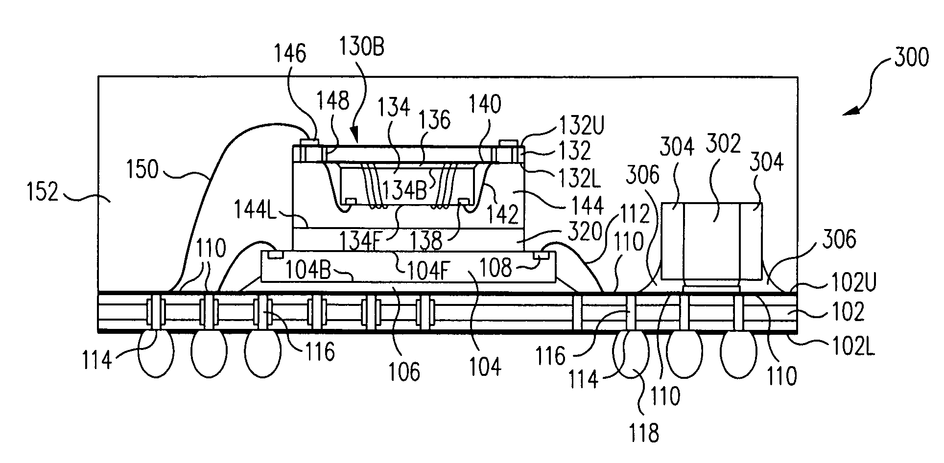
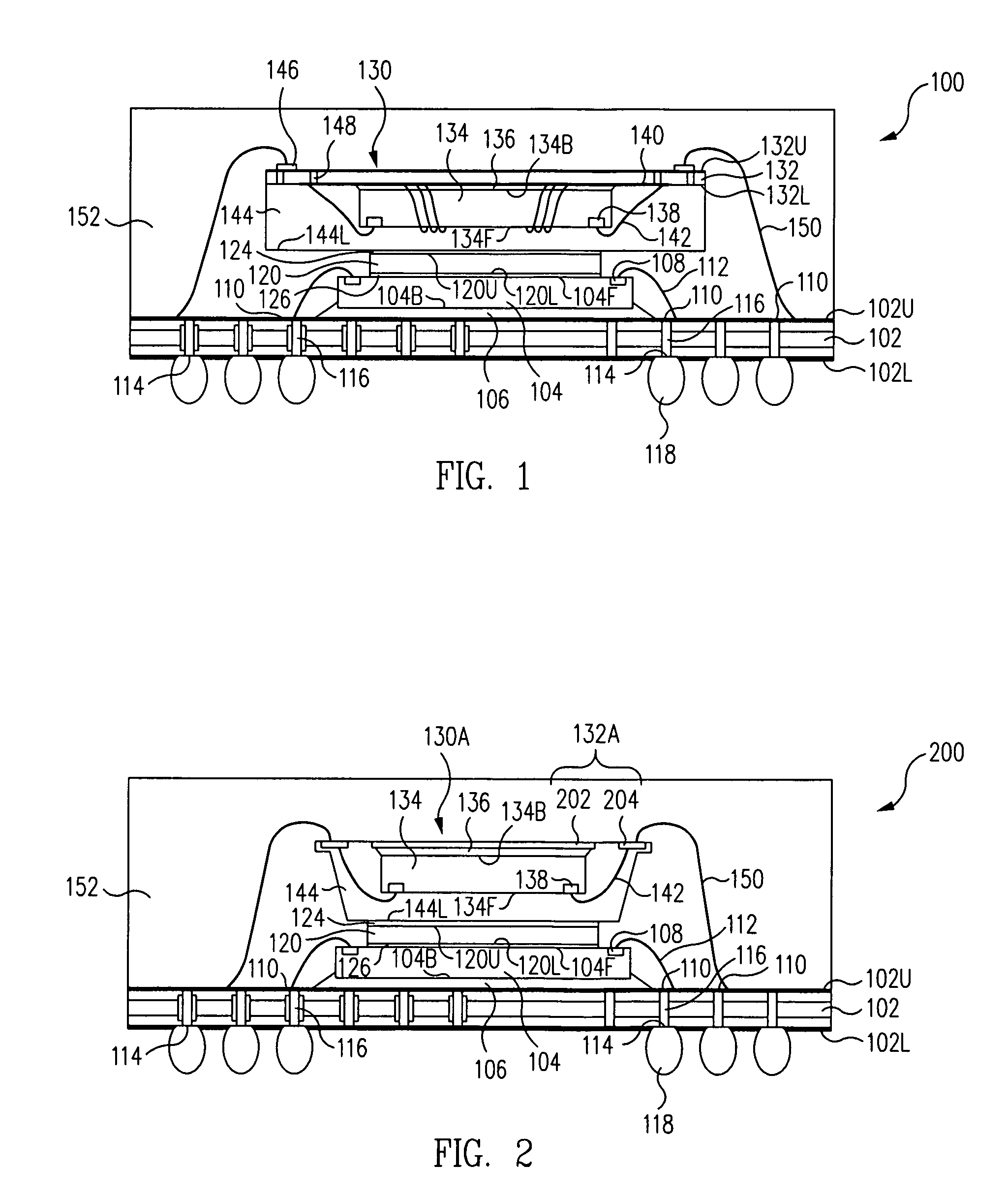
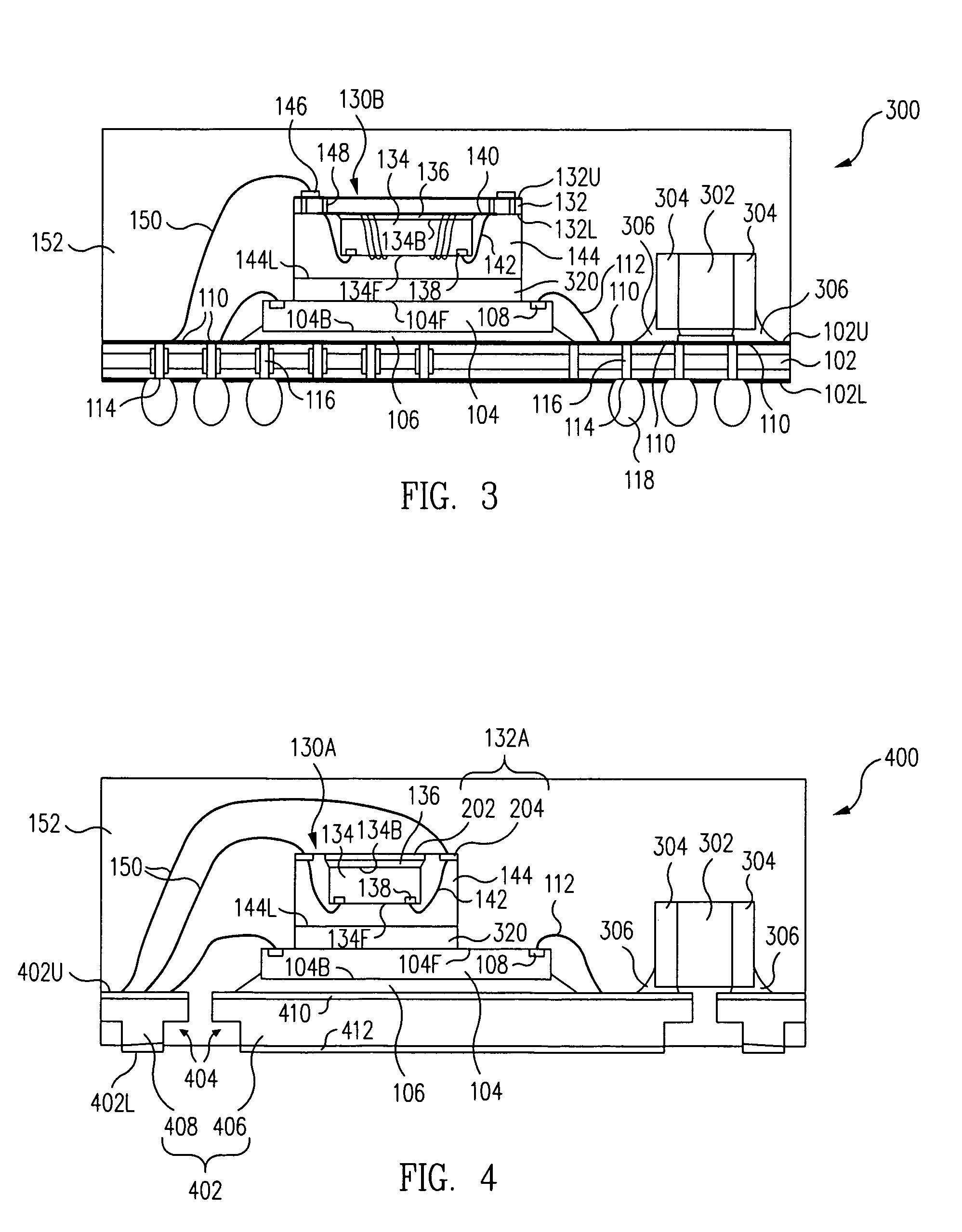
[0022]In accordance with one embodiment, a package 100 (FIG. 1) includes an internal package 130 stacked upon a primary die 104. Package 100 includes interconnection balls 118 to allow package 100 to be electrically and physically connected to a larger substrate, e.g., a printed circuit board, sometimes called a mother board. Thus, in contrast to stack mounting and electrically connecting a plurality of individual packages on the mother board, package 100 is mounted in a single operation thus minimizing labor and the associated manufacturing cost. Further, in one embodiment, package 100 is tested and verified to be non-defective prior to mounting to the mother board further minimizing manufacturing cost associated with reworking defective packages mounted to the mother board. Further, by mounting internal package 130 to a frontside surface 104F of primary die 104 using spacer 120, package 100 is extremely thin.

[0023]More particularly, FIG. 1 is a cross-sectional view of a Chip Scale...


PUM


Abstract

A package includes an internal package stacked upon a primary die. The package includes interconnection balls to allow the package to be electrically and physically connected to a mother board. The package is mounted to the mother board in a single operation thus minimizing labor and the associated manufacturing cost. Further, the package is tested and verified to be non-defective prior to mounting to the mother board.

Description

RELATED APPLICATIONS[0001]This application claims the benefit of U.S. Provisional Application No. 60 / 630,775 filed on Nov. 24, 2004, entitled “PACKAGE IN PACKAGE (PiP)” of Jon T. Woodyard, which is incorporated herein by reference in its entirety.BACKGROUND OF THE INVENTION[0002]1. Field of the Invention[0003]The present invention relates generally to the packaging of electronic components.[0004]2. Description of the Related Art[0005]To decrease the area required for mounting of electronic component packages to printed circuit boards, e.g., mother boards, electronic component packages are frequently stacked one upon another. However, stacking electronic component packages individually one upon another on the mother board is labor-intensive and thus significantly adds to the manufacturing cost. Further, after stacking of the electronic component packages, the stack of electronic component packages must be tested, e.g., for failure of the electrical connection, e.g., solder, between t...

Claims


Application Information

Patent Timeline
Patent Type & Authority Patents(United States)
IPC IPC(8): H01L23/02
CPCH01L23/49548H01L23/49575H01L25/03H01L25/0652H01L25/0657H01L23/3107H01L23/3128H01L23/49816H01L2224/32145H01L2224/48227H01L2224/48235H01L2224/48247H01L2224/73204H01L2224/73215H01L2224/73253H01L2224/73265H01L2225/0651H01L2225/06517H01L2225/06568H01L2924/01079H01L2924/09701H01L2924/15311H01L2924/19105H01L2924/19107H01L24/48H01L2224/16225H01L2224/32225H01L2224/32245H01L2924/00011H01L2924/00012H01L2924/00H01L24/73H01L2224/0557H01L2224/05573H01L2924/00014H01L2224/04042H01L2924/181H01L2224/05571H01L2224/0554H01L2224/05599H01L2224/45099H01L2224/45015H01L2924/207H01L2224/0555H01L2224/0556
Inventor WOODYARD, JON T.
Owner AMKOR TECH SINGAPORE HLDG PTE LTD
Why Eureka
Try Eureka