Method of fabricating photomask blank

a technology of photomask and photoplate, which is applied in the field of method of fabricating photoplate, can solve the problems of reducing manufacturing yield, affecting manufacturing yield, and reducing depth of focus, and achieves the effect of reducing stress

Active Publication Date: 2010-08-03
SHIN ETSU CHEM IND CO LTD
View PDF12 Cites 6 Cited by
  • Summary
  • Abstract
  • Description
  • Claims
  • Application Information

AI Technical Summary

Benefits of technology

[0021]The present invention is designed in view of the above problems. An object of the present invention is to provide a photomask blank comprising an optical film undergoing reduced stress and offering in-plane uniform optical properties.
[0027]According to the present invention, in the step of irradiating the optical film formed on a principle surface of the transparent substrate with flash light, the susceptor is used, which has the excavated portion that accommodates the transparent substrate and the sidewall portion surrounding the excavated portion. The sidewall portion partly constitutes the opaque area. The difference in height between the top surface of the opaque area and the top surface of the transparent substrate accommodated in the excavated portion has a predetermined value. Thus, during flash light irradiation, an area located close to an end of the substrate is inhibited from being excessively irradiated with flash light. This makes it possible to provide a photomask blank comprising an optical film undergoing reduced stress and offering in-plane uniform optical properties.

Problems solved by technology

On the other hand, as is apparent from Formula (2), shown above, the reduction in exposure wavelength is effective for a reduction in resolution pitch RP but reduces the depth of focus DOF, affecting manufacturing yield.
That is, in spite of the advantage of reducing the k factor to allow microstructures to be transferred, the reduction in exposure wavelength reduces the depth of focus DOF, resulting in a focus error and thus a decrease in manufacturing yield if the photomask is not sufficiently flat.
The distortion may reduce the overlapping accuracy of the photomask, causing defects in a circuit pattern to be drawn.
It is very difficult to control or release the stress during the process of fabricating a photomask.
However, it is very difficult and virtually impossible to find fabrication process conditions in which film formation conditions for providing appropriate properties for thin films used as optical films also serve as conditions for forming thin films with reduced stress.
However, stress may occur in the films during the film formation process and distort the substrate itself, warping the photomask blank.
However, owing to excessive energy application, resulting in an increase in substrate temperature, these techniques may damage the substrate itself or increase the time required for treatment.
This disadvantageously degrades productivity.
However, light irradiation using a flash lamp may increase the amount of light applied to an outer peripheral area of an optical film formed on the substrate above the amount of light applied to a central area due to reflection from a susceptor holding the substrate by a back surface of the substrate.
This unfortunately causes an in-plane variation in the optical properties of the films.

Method used


Image

  • Method of fabricating photomask blank
  • Method of fabricating photomask blank
  • Method of fabricating photomask blank

Examples


embodiment

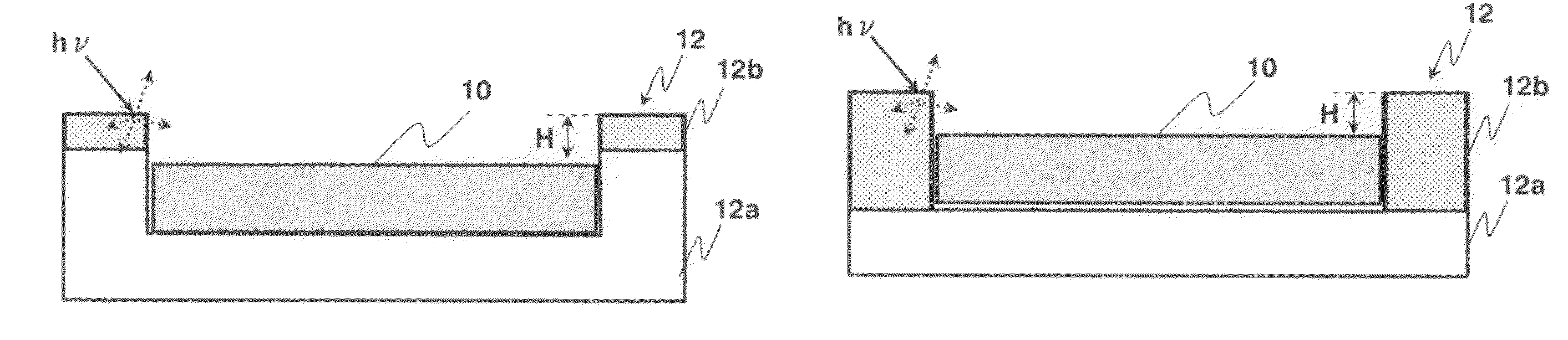
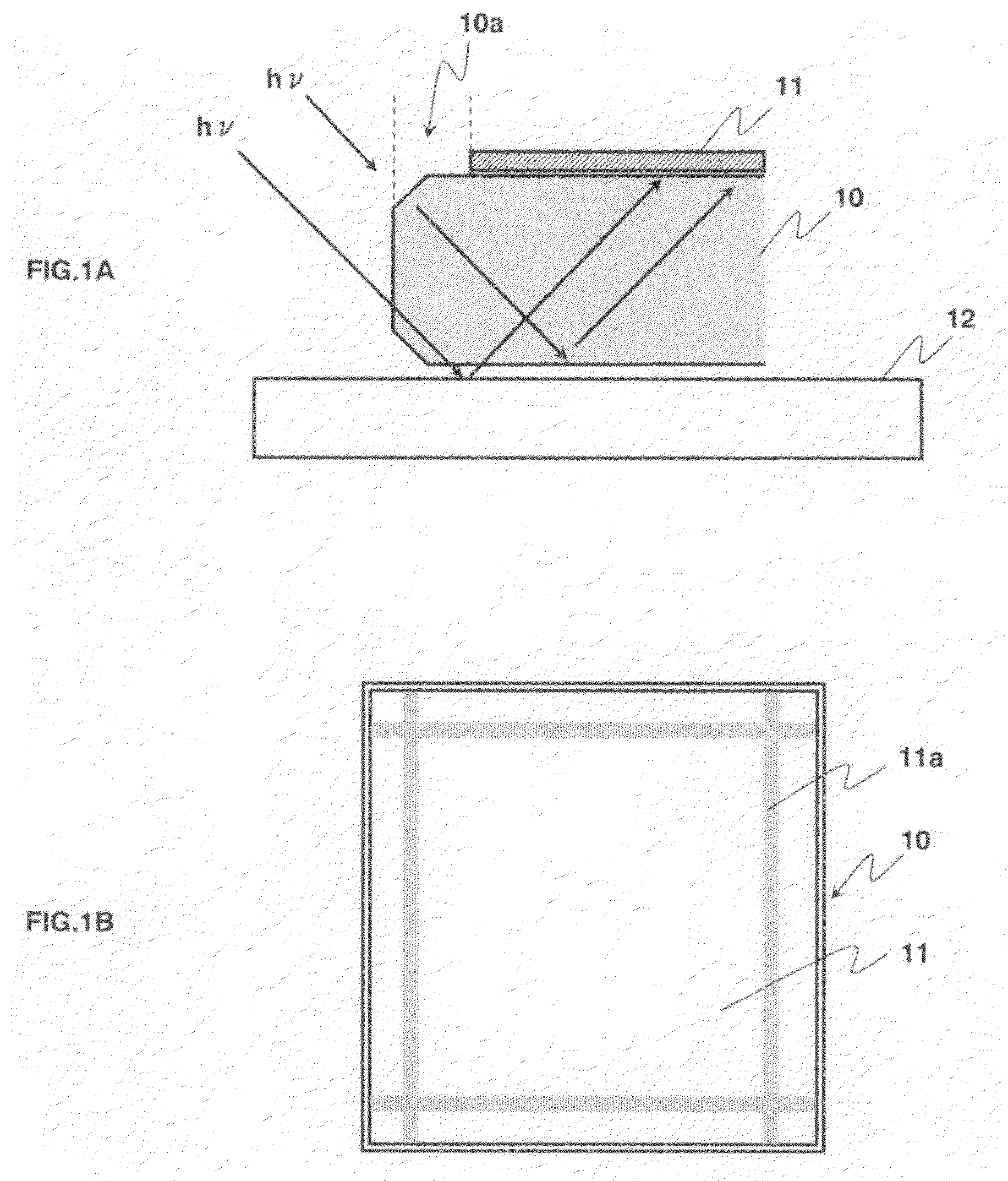
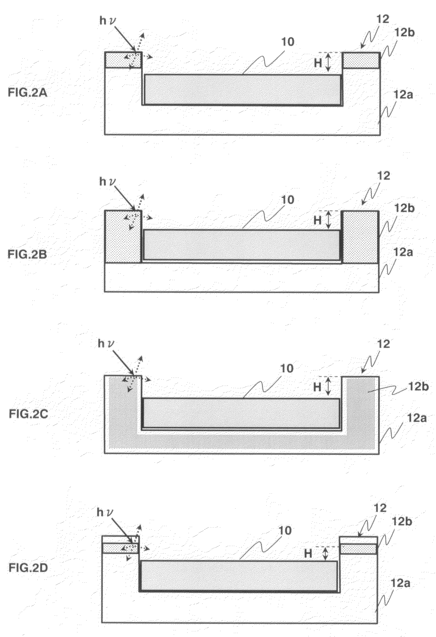
[0048]First, a halftone phase shift film of MoSiON was formed on a square quartz substrate of 6 inches square to a film thickness of 700 Å by reactive DC sputtering. The phase shift film exhibited a phase difference of 180° for exposure light from an ArF excimer laser (193 nm) and a transmittance equal to about 6% of that of a bare substrate. After being heated to 80° C., the substrate (that is, a substrate with a phase shift film) was placed on the susceptor with the excavated portion so that the phase shift film faces upward. The substrate was irradiated, from above, with light from the xenon flash lamp. At this time, susceptors of the type shown in FIG. 2C which have different excavation heights (that is, the heights of the sidewall portions of the susceptors) were prepared. Flash light irradiation was performed using each of the susceptors.

[0049]FIG. 3 is a diagram showing an in-plane variation in the transmittance of the halftone phase shift film observed after flash light irra...


PUM

PropertyMeasurementUnit
heightaaaaaaaaaa
wavelengthaaaaaaaaaa
transmittanceaaaaaaaaaa

Abstract

An opaque area is formed in a sidewall portion of a susceptor by stacking a material that is transparent to flash light and a material that is opaque to the flash light to form the sidewall portion or coating a surface of the opaque material with the transparent material. A top surface of the opaque area in the sidewall portion of the susceptor is designed to have a predetermined positional relationship with a top surface of a substrate; the top surface of the opaque area is set at the same position as that of the top surface of the substrate or higher than the top surface of the substrate by a predetermined height. Thus, obliquely incident flash light is absorbed or irregularly reflected by the opaque quartz portion, surrounding an excavated portion of the susceptor.

Description

BACKGROUND OF THE INVENTION[0001]1. Field of the Invention[0002]The present invention relates to a method of fabricating a photomask blank, and more specifically, to a technique of fabricating a photomask blank as a material for a photomask used to micromachine semiconductor integrated circuits, CCDs (Charged-Coupled Devices), color filters for LCD (Liquid Crystal Display) devices, magnetic heads, and the like.[0003]2. Description of the Related Art[0004]Lithography techniques are used to, for example, fabricate semiconductor integrated circuits, which have been increasingly highly integrated. For the lithography techniques, efforts have been made to reduce the wavelength of exposure light used for light exposure apparatuses in order to improve resolution. According to a road map for lithography updated by ITRS (International Technology for Semiconductors) in 2004, the reduction in wavelength has progressed from a g line (wavelength λ=436 nm) and an i line (λ=365 nm) which are ultra...

Claims


Application Information

Patent Timeline
Patent Type & Authority Patents(United States)
IPC IPC(8): G03F1/00G03F1/26G03F1/68
CPCG03F1/32G03F1/08G03F1/50G03F1/26G03F1/38
Inventor FUKUSHIMA, NORIYASUYOSHIKAWA, HIROKI
Owner SHIN ETSU CHEM IND CO LTD
Why Eureka
Try Eureka