Method for driving a liquid crystal display

Active Publication Date: 2010-08-03
AU OPTRONICS CORP
View PDF6 Cites 12 Cited by
  • Summary
  • Abstract
  • Description
  • Claims
  • Application Information

AI Technical Summary

Benefits of technology

[0016]A method for driving a normal black or white liquid crystal display (LCD) is provided. The LCD comprises a liquid crystal layer, a thin film transistor (TFT), a pixel electrode, and a counter electrode. The TFT comprises a source receiving a

Problems solved by technology

It is difficult to remove such electrical field, and thus an image sticking issue arises in the panel resulting in image distortion.
The '549 patent, however, do

Method used


Image

  • Method for driving a liquid crystal display
  • Method for driving a liquid crystal display
  • Method for driving a liquid crystal display

Examples


Embodiment Construction

[0034]The following description is of the best-contemplated mode of carrying out the invention. This description is made for the purpose of illustrating the general principles of the invention and should not be taken in a limiting sense. The scope of the invention is determined by reference to the appended claims.

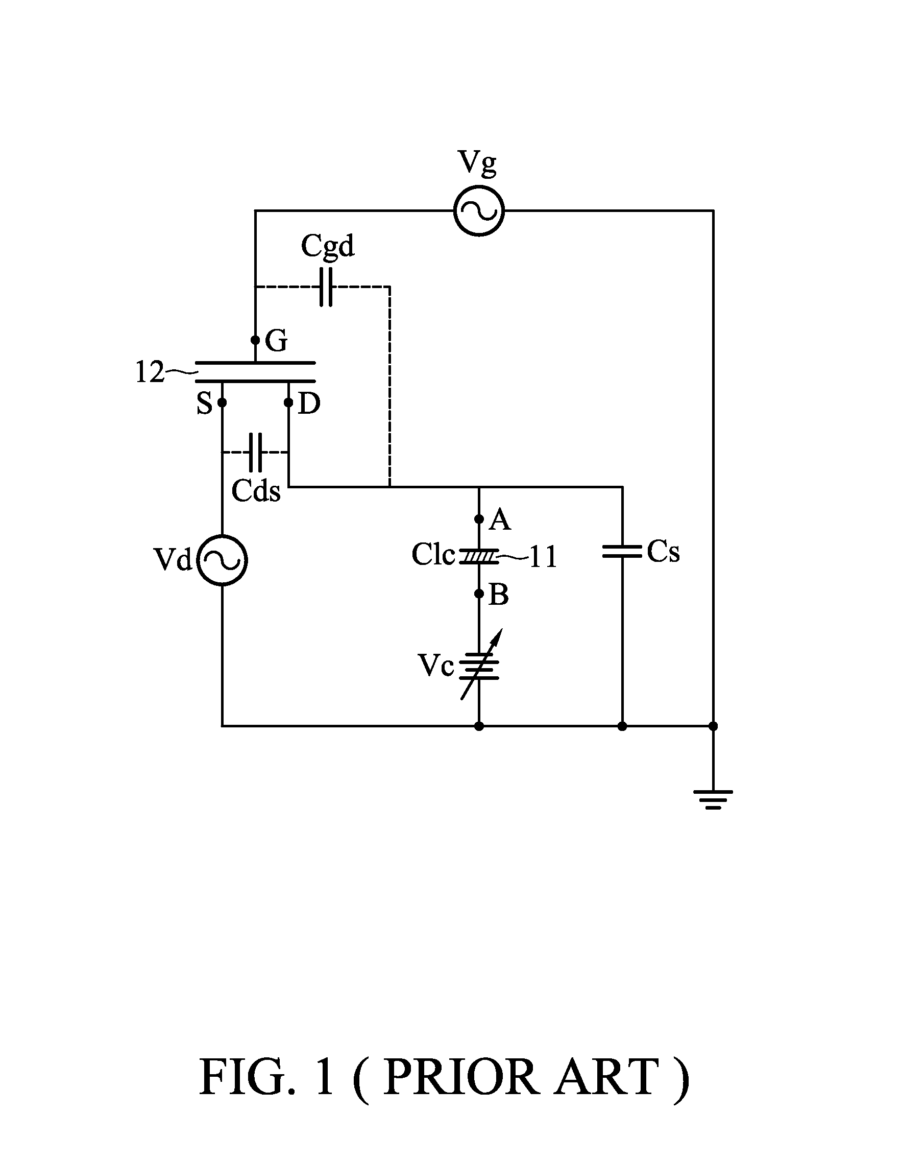
[0035]The invention provides a method for driving an LCD according to the layouts of a driving circuit, materials of a liquid crystal layer, changes of the leading axle of the liquid crystal and characteristics of positive or negative ions. The method for driving an LCD, according to the present invention, can be implemented for reducing image sticking. Taking the LCD shown in FIG. 1 and FIGS. 4A to 4F as an example, the operating principle of the method for driving an LCD is described in the following

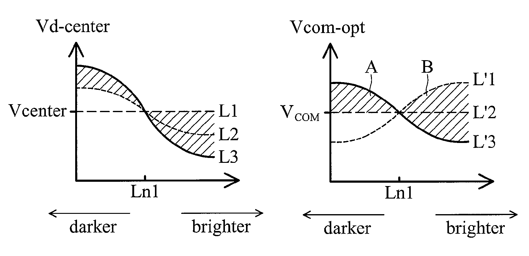
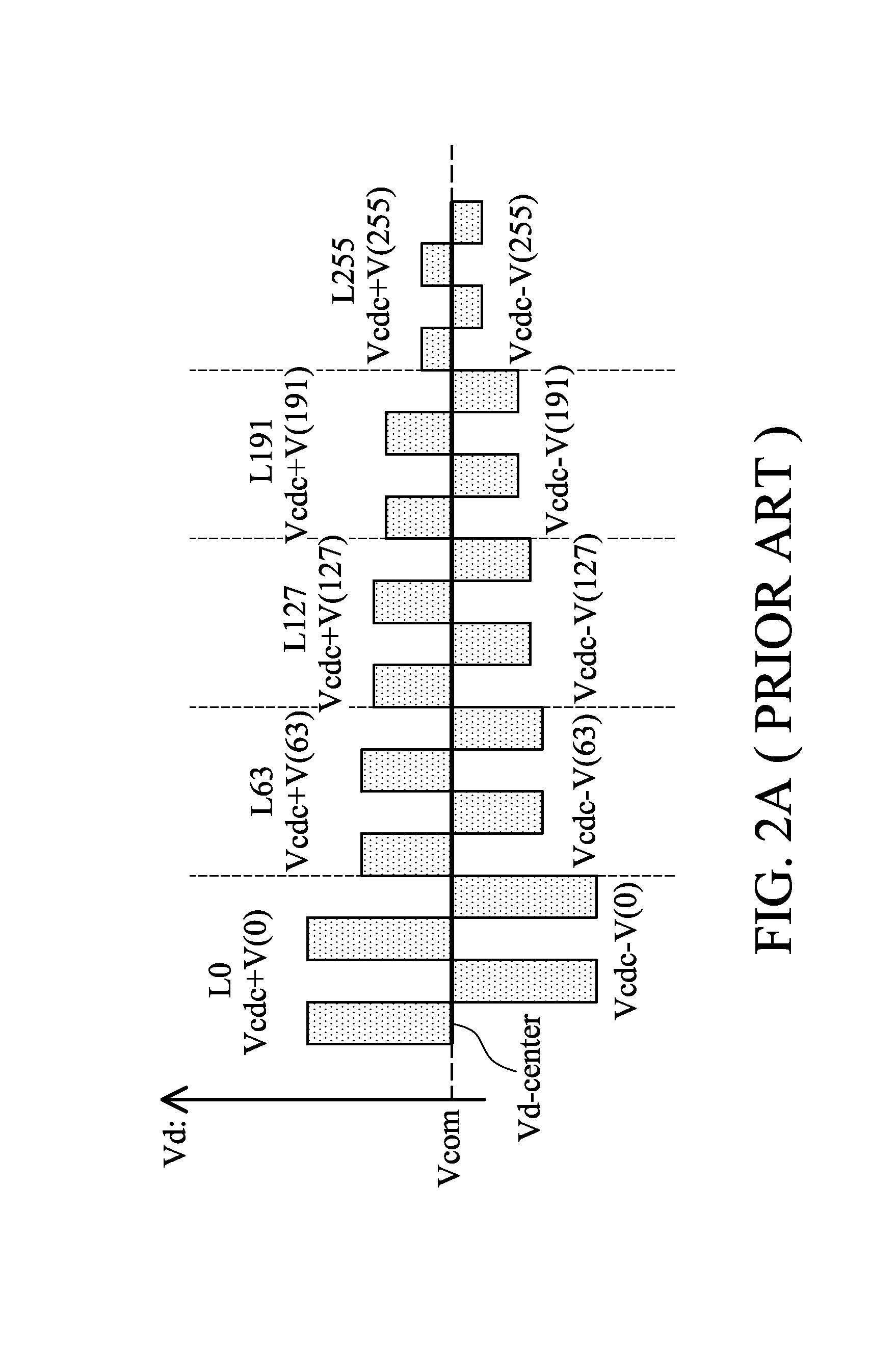
[0036]FIG. 4A shows a relationship curve L1 between the middle-voltage Vd_center of the source signal Vd and the gray levels (various source signals) when the source signal Vd...


PUM


Abstract

A method for driving a normal black type liquid crystal display (LCD) includes driving the LCD by applying uncompensated source signals corresponding to gray levels; recording first optimized common signal voltages (Vcom-opt1) of common signals corresponding with the gray levels; adjusting the source signal to drive the LCD so second optimized common signal voltages (Vcom-opt2) of common signals corresponding with the gray levels conform to the following conditions: (1) when the gray level is lower than a predetermined gray level, the Vcom-opt2 exceeds a predetermined voltage of the common signal and the absolute difference between the Vcom-opt2 and the predetermined voltage is less than or equal to that between the Vcom-opt1 and the predetermined voltage; and (2) when the gray level exceeds the predetermined gray level, the absolute difference between the Vcom-opt2 and the predetermined voltage is less than or equal to that between the Vcom-opt1 and the predetermined voltage.

Description

BACKGROUND OF THE INVENTION[0001]1. Field of the Invention[0002]The invention relates to a liquid crystal display, and more particularly, to a method for eliminating image sticking in an LCD.[0003]2. Description of the Related Art[0004]FIG. 1 is a schematic diagram of a pixel and a driving circuit of a panel. The panel comprises a liquid crystal layer 11 disposed between a pixel electrode A (not shown) formed on a first substrate and a counter electrode (not shown) formed on a second substrate. A thin film transistor (TFT) 12 is disposed on the first substrate. A gate G of TFT 12 is electrically coupled to a gate line of the first substrate and a source S of TFT 12 is electrically coupled to a source line of the first substrate. Pixel electrode A is coupled to a drain D of TFT 12. Counter electrode B is coupled to a common signal source providing a common signal VC.[0005]The source line is coupled to a source signal source providing various source signals Vd for adjusting the voltag...

Claims


Application Information

Patent Timeline
IPC IPC(8): G09G3/36G06F3/038
CPCG09G3/3648G09G2320/0204G09G2320/0219
Inventor LIU, PIN-MIAOTSAO, CHENG-HANCHEN, PO-LUN
Owner AU OPTRONICS CORP
Why Eureka
Try Eureka