Electrical connector with complementary conductive elements

a technology of electrical connectors and complementary conductive elements, which is applied in the direction of printed circuit assembling, coupling device connection, printed circuit manufacturing, etc., can solve the problems of electrical interference between adjacent signal conductors, large size of electronic systems, and faster and functionally more complex electrical systems, so as to improve the integrity of electrical connectors.

Active Publication Date: 2010-09-14
AMPHENOL CORP
View PDF70 Cites 122 Cited by
  • Summary
  • Abstract
  • Description
  • Claims
  • Application Information

AI Technical Summary

Benefits of technology

[0010]Signal integrity in an electrical connector may be improved by forming adjacent conductive elements with complimentary shapes. Conductive elements containing projections are positioned adjacent conductive elements with relieved portions. Such a configuration of conductive elements contributes to a more uniform conductor to conductor spacing, which may impart conductive elements carrying signals with desirable electrical properties.

Problems solved by technology

Electronic systems have generally become smaller, faster and functionally more complex.
One of the difficulties in making a high density, high speed connector is that electrical conductors in the connector can be so close that there can be electrical interference between adjacent signal conductors.

Method used


Image

  • Electrical connector with complementary conductive elements
  • Electrical connector with complementary conductive elements
  • Electrical connector with complementary conductive elements

Examples


Embodiment Construction

[0024]This invention is not limited in its application to the details of construction and the arrangement of components set forth in the following description or illustrated in the drawings. The invention is capable of other embodiments and of being practiced or of being carried out in various ways. Also, the phraseology and terminology used herein is for the purpose of description and should not be regarded as limiting. The use of “including,”“comprising,”“having,”“containing,” or “involving,” and variations thereof herein, is meant to encompass the items listed thereafter and equivalents thereof as well as additional items.

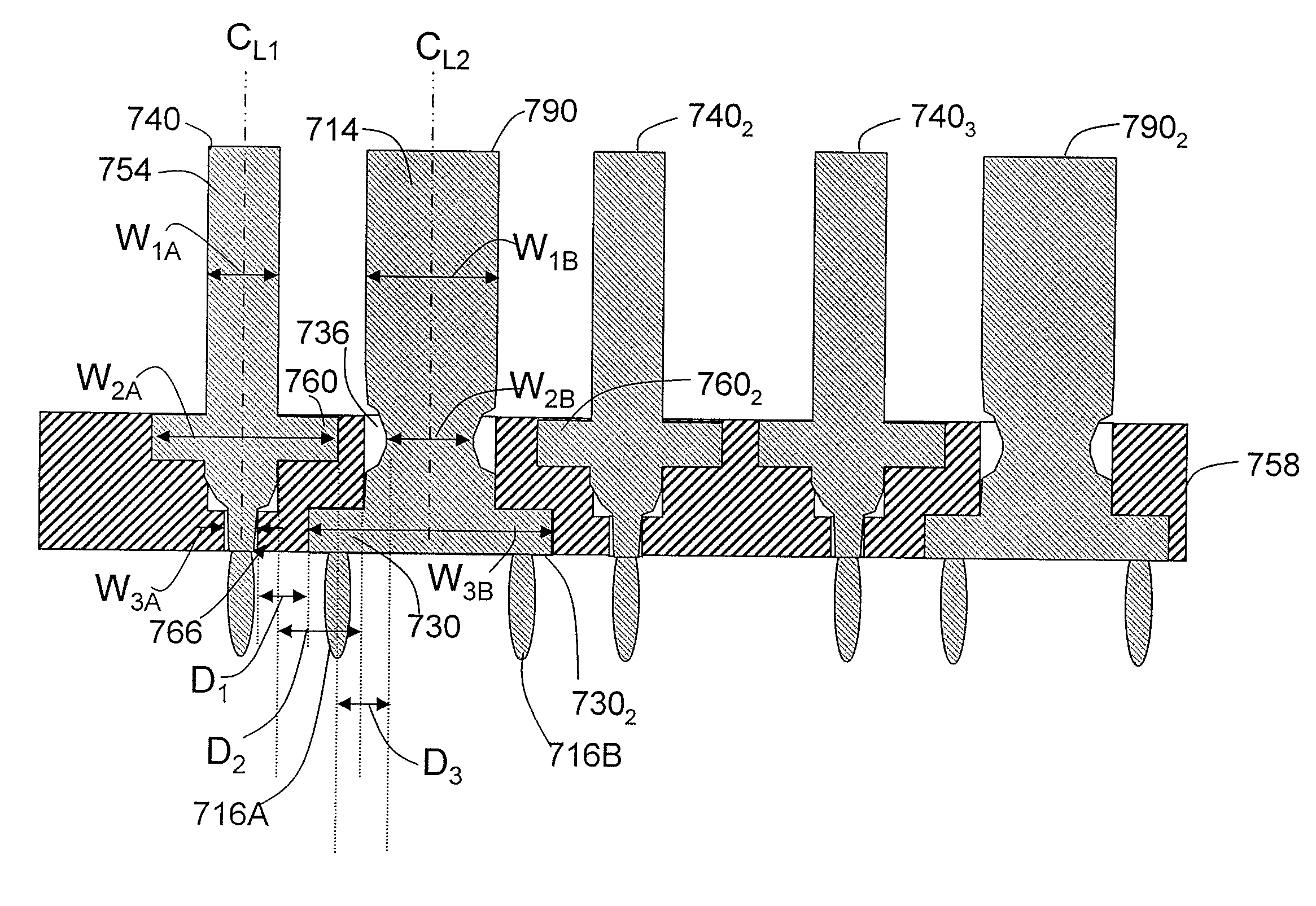
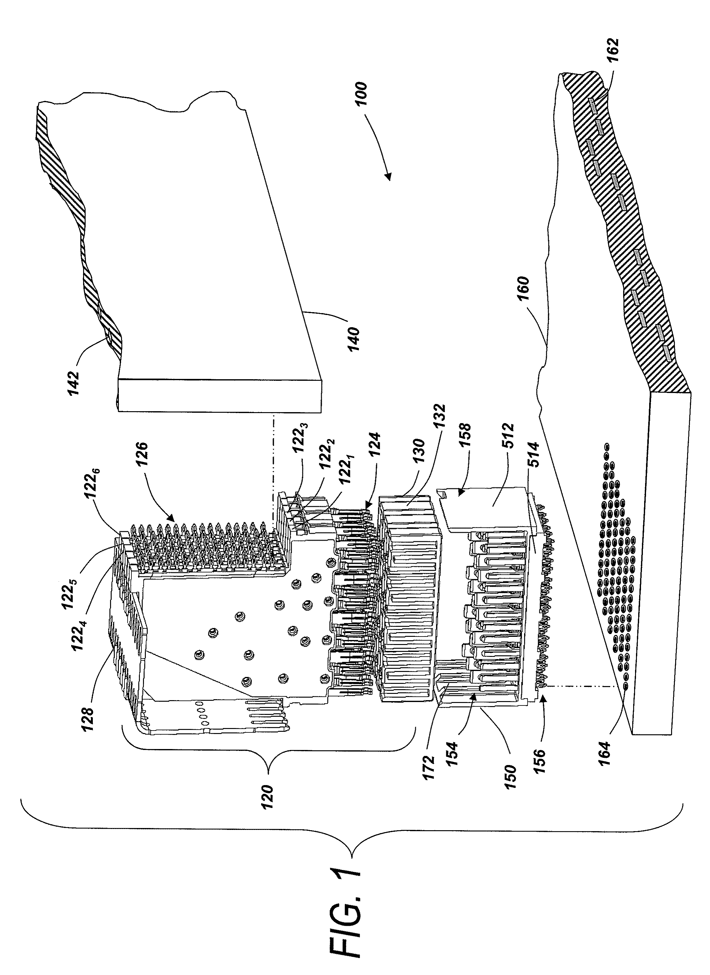
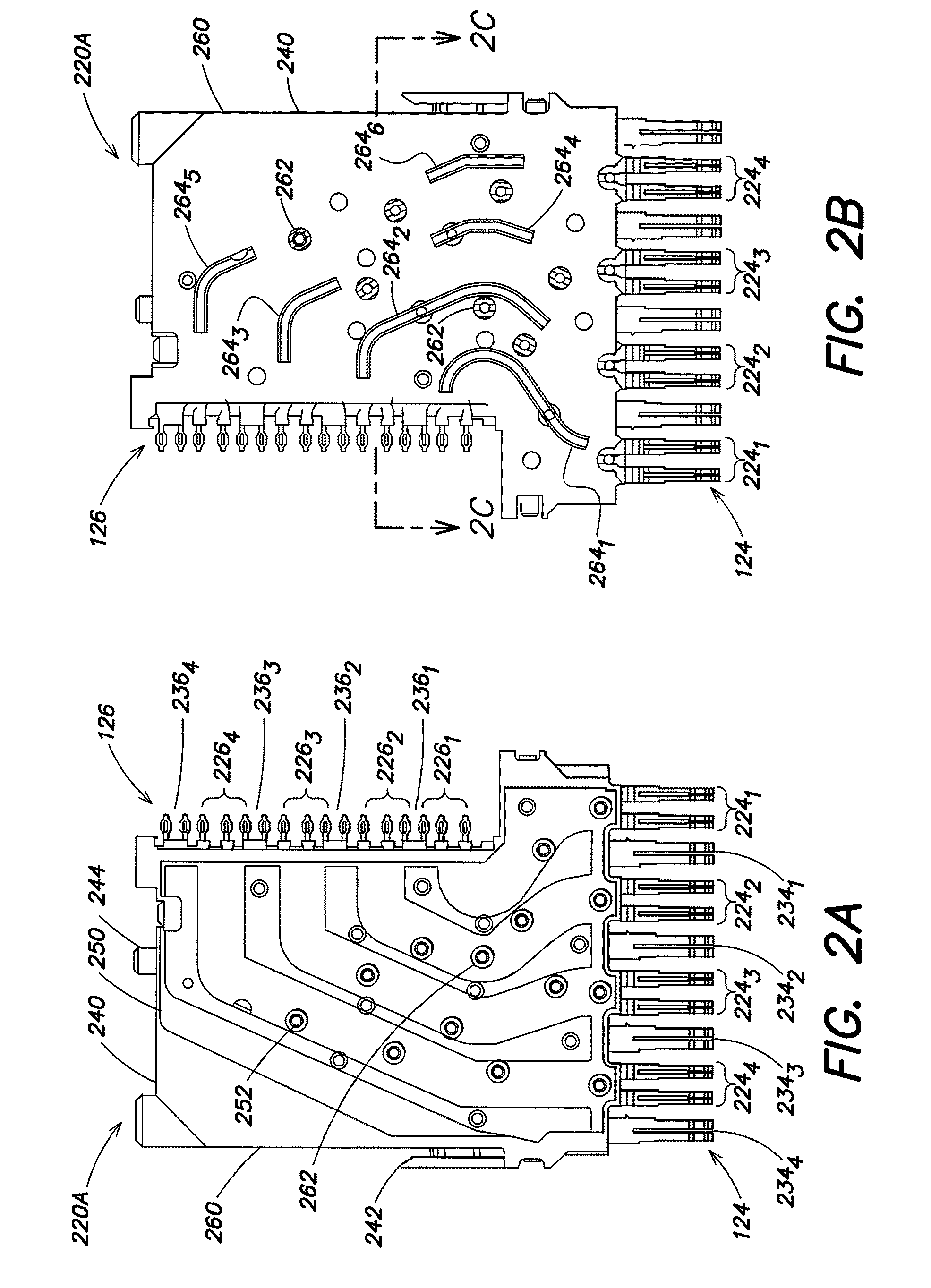
[0025]Referring to FIG. 1, an electrical interconnection system 100 with two connectors is shown. The electrical interconnection system 100 includes a daughter card connector 120 and a backplane connector 150.

[0026]Daughter card connector 120 is designed to mate with backplane connector 150, creating electronically conducting paths between backplane 160 and daug...


PUM

PropertyMeasurementUnit
dielectric constantaaaaaaaaaa

Abstract

An electrical interconnection system with high speed, differential electrical connectors. The connectors are formed with columns of conductive elements, some of which carry signals some of which act as ground conductors. The conductive elements may contain projections to secure the conductive elements in a housing or to facilitate desirable current flow patterns. To avoid impedance discontinuities caused by the projections, adjacent conductive elements may be formed with complementary portions to provide a relatively uniform edge-to-edge spacing between signal and ground conductors along the length of the signal conductor. To manufacture such a connector in which both the signal and the ground conductive elements contain projections, the conductive elements carrying signals may be inserted into a housing from one side and the conductive elements acting as ground conductors may be inserted from an opposite side.

Description

CROSS-REFERENCE TO RELATED APPLICATIONS[0001]This application claims priority to U.S. Provisional Application 60 / 921,696, filed Apr. 4, 2007 and incorporated herein by reference.BACKGROUND OF INVENTION[0002]1. Field of Invention[0003]This invention relates generally to electrical interconnection systems and more specifically to improved signal integrity in interconnection systems, particularly in high speed electrical connectors.[0004]2. Discussion of Related Art[0005]Electrical connectors are used in many electronic systems. It is generally easier and more cost effective to manufacture a system on several printed circuit boards (“PCBs”) that are connected to one another by electrical connectors than to manufacture a system as a single assembly. A traditional arrangement for interconnecting several PCBs is to have one PCB serve as a backplane. Other PCBs, which are called daughter boards or daughter cards, are then connected through the backplane by electrical connectors.[0006]Elect...

Claims


Application Information

Patent Timeline
Patent Type & Authority Patents(United States)
IPC IPC(8): H01R12/00
CPCH01R13/65807H01R12/727H01R13/6477H01R13/6587H01R13/6471Y10T29/49126
Inventor COHEN, THOMAS S.KIRK, BRIAN
Owner AMPHENOL CORP
Why Eureka
Try Eureka