Source/drain carbon implant and RTA anneal, pre-SiGe deposition

a source/drain carbon implant and anneal technology, applied in the field of source/drain carbon implants and rta anneal, pre-sige deposition, can solve the problems of creating a uni-axial compressive stress within the channel region, damage to the sidewalls and bottom of the recessed source/drain region, and boron may tend to out-diffuse into, so as to reduce the induced barrier lowering, and improve the short channel

Active Publication Date: 2010-11-23
TAIWAN SEMICON MFG CO LTD
View PDF8 Cites 25 Cited by
  • Summary
  • Abstract
  • Description
  • Claims
  • Application Information

AI Technical Summary

Benefits of technology

[0007]Advantages of preferred embodiments of the present invention may include providing an improved short channel effect demonstrated by a thirty percent lower drain induced barrier lowering (DIBL). A further advantage of an illustrative embodiment of the present invention is reduced gate edge damage from a reduced pocket implant. Yet another advantage of an illustrative embodiment of the present invention is a lower e-SiGe resistance.

Problems solved by technology

In this case, lattice mismatch creates a uni-axial compressive stress within the channel region.
One problem facing complementary metal-oxide-semiconductor (CMOS) manufacturing is that N-channel metal-oxide-semiconductor (NMOS) and P-channel metal-oxide-semiconductor (PMOS) devices require different types of stress in order to achieve increased carrier mobility.
However, because of the high concentration of boron in the e-SiGe, the boron may tend to out-diffuse into the channel region.
One disadvantage to the known method is that the pocket implant dose may be high enough to cause damage to the sidewalls and bottom of the recessed source / drain regions, in which the stressor material layer or layers are deposited.
A further disadvantage to the known methods and structures is that boron out-diffusion is not adequately controlled, resulting in short channel effects.

Method used


Image

  • Source/drain carbon implant and RTA anneal, pre-SiGe deposition
  • Source/drain carbon implant and RTA anneal, pre-SiGe deposition
  • Source/drain carbon implant and RTA anneal, pre-SiGe deposition

Examples


Embodiment Construction

[0020]The making and using of the presently preferred embodiments are discussed in detail below. It should be appreciated, however, that an illustrative embodiment provides many applicable inventive concepts that can be embodied in a wide variety of specific contexts. The specific embodiments discussed are merely illustrative of specific ways to make and use the invention, and do not limit the scope of the invention.

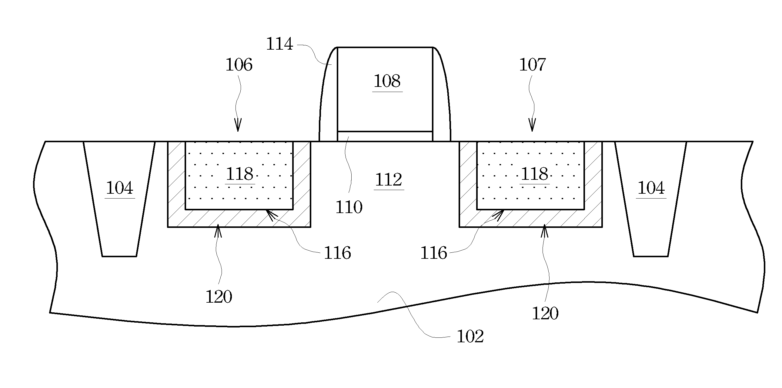
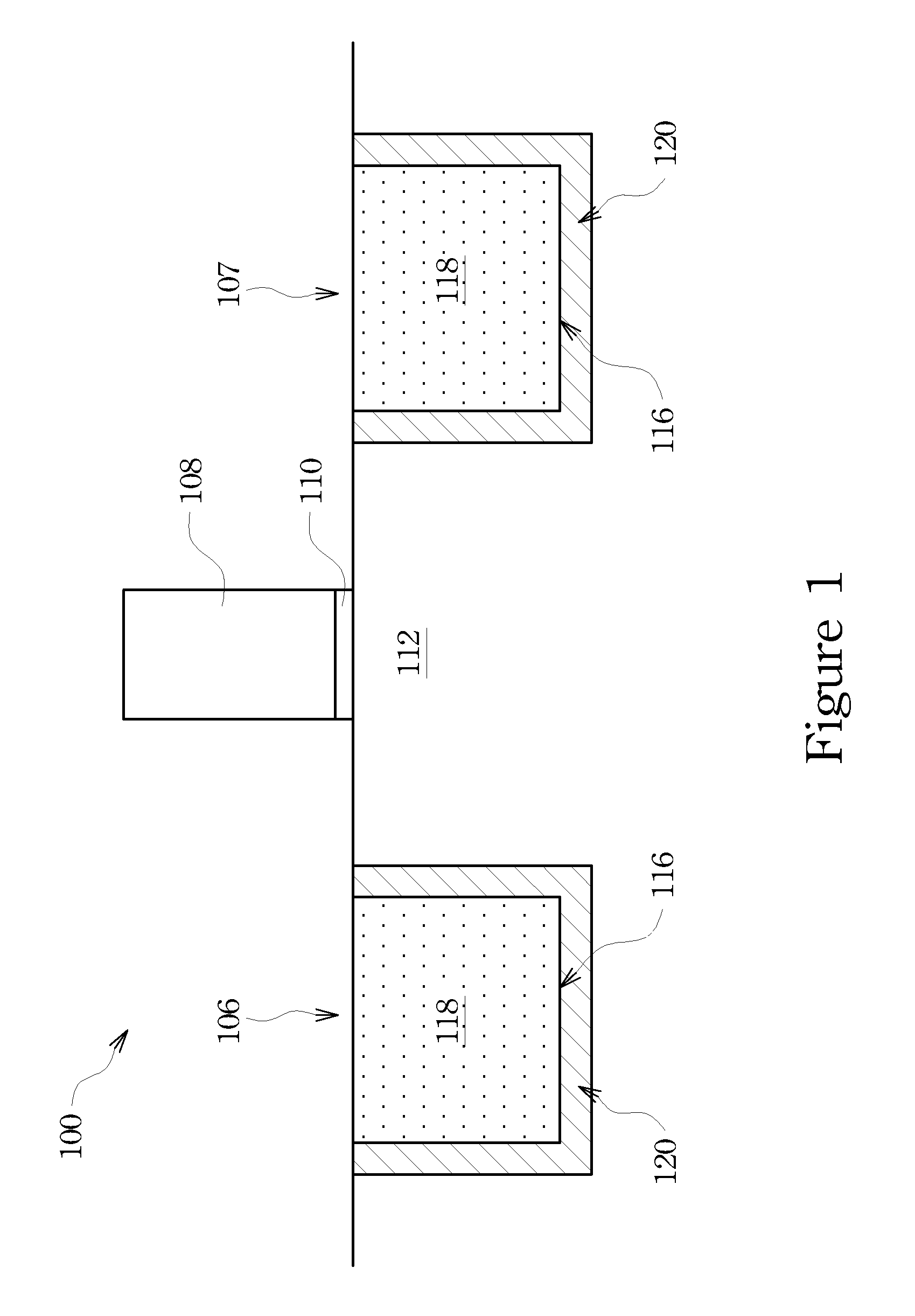
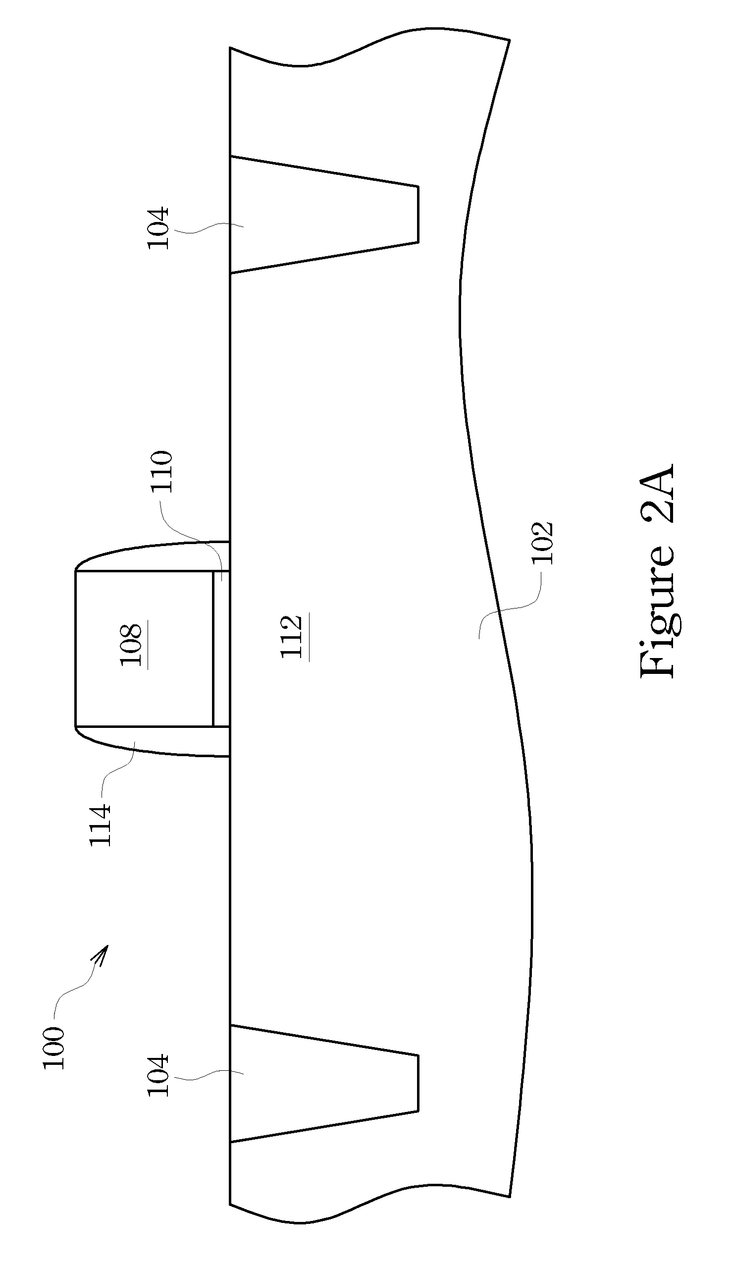
[0021]The present invention will be described with respect to illustrative embodiments in a specific context, namely boron doped, epitaxially grown, SiGe embedded source / drain PMOS transistor. The invention may also be applied, however, to other semiconductor devices including other stressor materials, for example Si doped with Sb and the like. Further, the example barrier dopant in the embodiment illustrated is carbon; other barrier dopants are within the scope of the invention including but not limited to fluorine, nitrogen and the like.

[0022]FIG. 1 depicts a cross-sec...


PUM


Abstract

A semiconductor device system, structure, and method of manufacture of a source / drain to retard dopant out-diffusion from a stressor are disclosed. An illustrative embodiment comprises a semiconductor substrate, device, and method to retard sidewall dopant out-diffusion in source / drain regions. A semiconductor substrate is provided with a gate structure, and a source and drain on opposing sides of the gate structure. Recessed regions are etched in a portion of the source and drain. Doped stressors are embedded into the recessed regions. A barrier dopant is incorporated into a remaining portion of the source and drain.

Description

TECHNICAL FIELD[0001]The present invention relates generally to a semiconductor device, system, and method of manufacture, and more particularly to a semiconductor device, system, and method to retard dopant out-diffusion in transistor source / drain regions.BACKGROUND[0002]Size reduction of metal-oxide-semiconductor field-effect transistors (MOSFET) has enabled the continued improvement in speed, performance, density, and cost per unit function of integrated circuits. One way to improve transistor performance is through selective application of stress to the transistor channel region. Stress distorts (i.e., strains) the semiconductor crystal lattice, and the distortion, in turn, affects the band alignment and charge transport properties of the semiconductor. By controlling the magnitude and distribution of stress in a finished device, manufacturers can increase carrier mobility and improve device performance.[0003]One approach of introducing stress in the transistor channel region in...

Claims


Application Information

Patent Timeline
Patent Type & Authority Patents(United States)
IPC IPC(8): H01L21/00
CPCH01L21/26506H01L21/26586H01L29/66636H01L29/7848H01L29/165H01L29/6653
Inventor WOON, WEI-YENNIEH, CHUN-FENGCHEN, CHING-YICHANG, HSUNYANG, CHUNG-RULIN, LI-TE S.
Owner TAIWAN SEMICON MFG CO LTD
Why Eureka
Try Eureka