Radiation imaging element

a radiation imaging and element technology, applied in the direction of radiation intensity measurement, instruments, x/gamma/cosmic radiation measurement, etc., can solve the problems of difficult to form transistors directly on resin substrates, low heat resistance, and increased radiation exposure, etc., to achieve excellent performance, small size, and large electric conductivity

Active Publication Date: 2010-12-21
SAMSUNG DISPLAY CO LTD
View PDF17 Cites 35 Cited by
  • Summary
  • Abstract
  • Description
  • Claims
  • Application Information

AI Technical Summary

Benefits of technology

[0105]The obtained TFT characteristics are shown in Table 2. It is shown in Table 2 that the inventive TFT element Nos. 1 and 2 exhibit excellent performance such as large field effect mobility and high ON-OFF ratio. On the contrary, the comparative TFT element No. 1, which has a configuration with only one active layer having moderate electric conductivity, exhibits small field effect mobility. The comparative TFT element No. 2, which includes a first active layer having small electric conductivity and a second active layer having large electric conductivity, exhibits extremely low ON-OFF ratio. The inventive TFT element Nos. 3 and 4 also show excellent effects of the invention.
[0106]As is clear from the above results, it is revealed that, by a configuration of the invention including a first active layer having large electric conductivity and a second active layer having small electric conductivity, unexpectedly excellent performance such as large field effect mobility and high ON-OFF ratio is obtained.
[0107]TABLE 2Gate Electrode / First Active LayerSecond Active LayerElement PerformanceElementThicknessDepositionThicknessDepositionThicknessMobilityON-OFFNo.Substrate(nm)Condition(nm)Condition(nm)(cm2 / Vs)RatioInventiveGlassITO / 30Condition 210Condition 44015.31.4 × 106Element No. 1InventiveGlassITO / 30Condition 110Condition 44017.22.7 × 106Element No. 2ComparativeGlassITO / 30Condition 350——4.39.0 × 105Element No. 1ComparativeGlassITO / 30Condition 410Condition 1404.21.4Element No. 2InventiveGlassMo / 40Condition 230Condition 52033.23.4 × 106Element No. 3InventivePENMo / 40Condition 110Condition 44021.12.2 × 106Element No. 4Example 2
[0108]Using the inventive or comparative thin film field effect transistor prepared in

Problems solved by technology

However, a direct conversion type radiation imaging element involves a large amount of noise, and therefore, an exposure amount of radiation has to be increased in order to obtain a high quality image, which is a problem.
However, fabrication of the transistors using thin films of silicon described above requires a thermal treatment process at a relatively high temperature, and it is difficult to form the transistors directly on a resin substrate which is generally low in heat resistance.
However, in the case of using a TFT formed using a-IGZO, as, for example, a drive circuit of a display, there are problems in that mobility ranges from 1 cm2 / Vs to 10 cm2 / Vs, which provides insufficient performance, the OFF current is high, and the ON-OFF ratio is low.

Method used


Image

  • Radiation imaging element
  • Radiation imaging element
  • Radiation imaging element

Examples


example 1

1. Preparation of Active Layer

[0071]

[0072]Using a polycrystalline sintered body having a composition of InGaZnO4 as a target, RF magnetron sputtering vacuum deposition was performed under the following conditions: flow rate of argon (Ar) of 12 sccm, flow rate of oxygen (O2) of 0.2 sccm, RF power of 200 W, and pressure of 0.4 Pa.

[0073]

[0074]Deposition was performed under similar conditions to those in the Condition 1 except that the flow rate of O2 was changed to 1.2 sccm.

[0075]

[0076]Deposition was performed under similar conditions to those in the Condition 1 except that the flow rate of O2 was changed to 1.4 sccm.

[0077]

[0078]Deposition was performed under similar conditions to those in the Condition 1 except that the flow rate of O2 was changed to 1.5 sccm.

[0079]

[0080]Deposition was performed under similar conditions to those in the Condition 1 except that the flow rate of O2 was changed to 1.8 sccm.

[0081]Samples for measurement of physical properties were prepared under the same c...

example 2

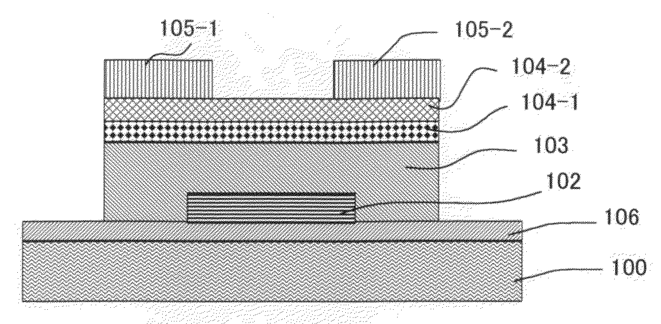
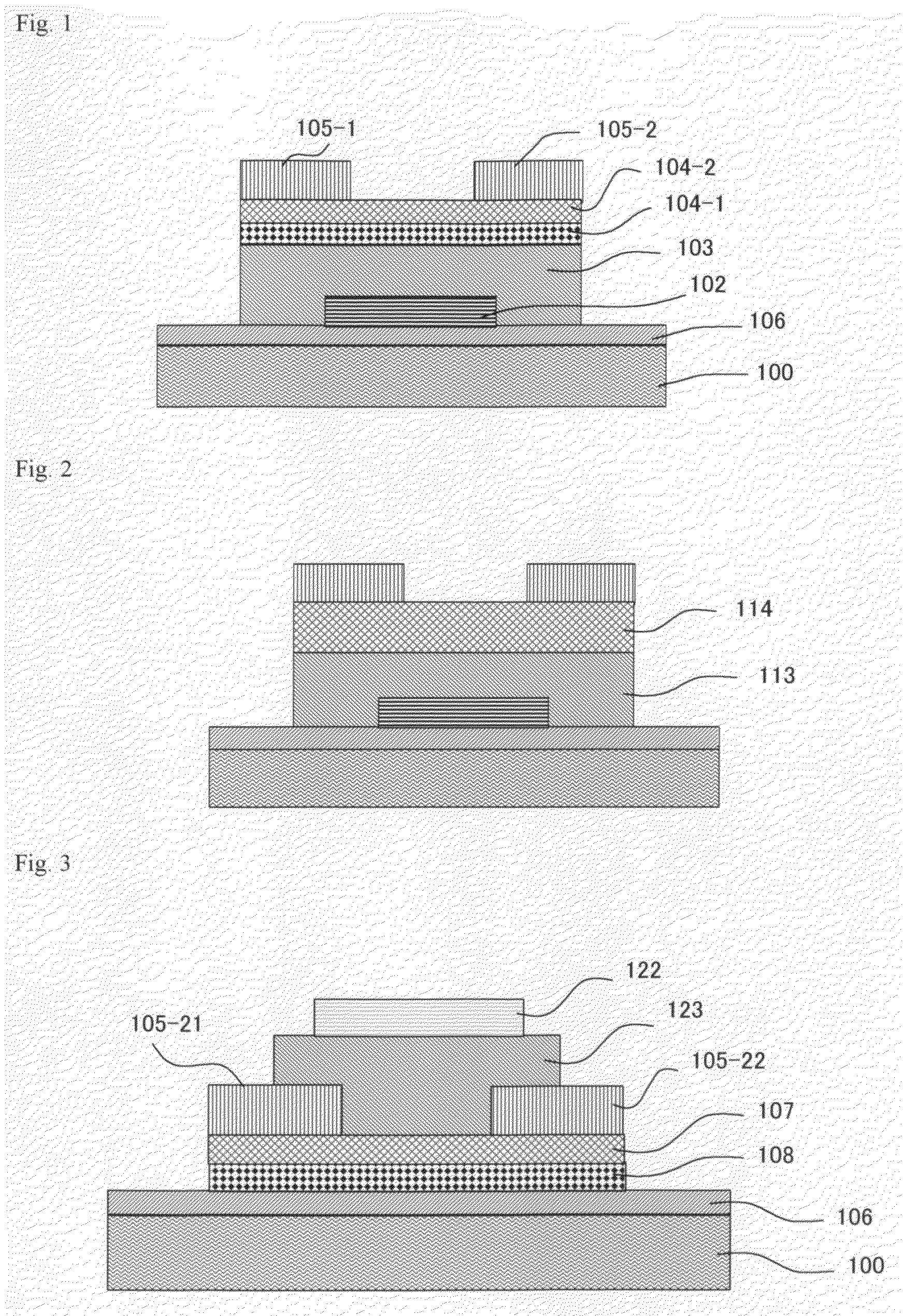
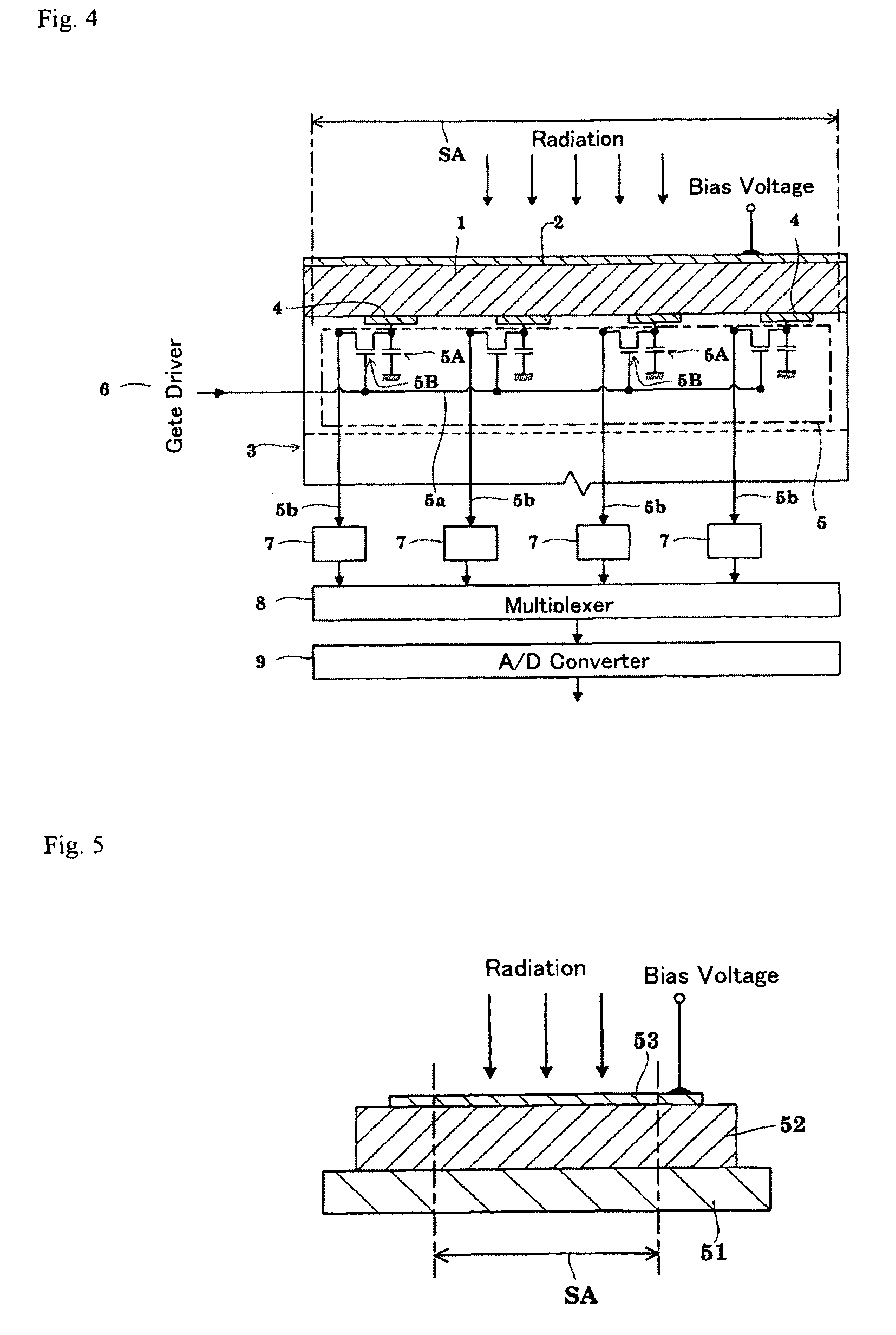
[0108]Using the inventive or comparative thin film field effect transistor prepared in Example 1, radiation imaging elements shown in FIG. 4 were fabricated. The performance of each of the obtained radiation imaging elements was evaluated. As a result, reflecting the performance of the thin film field effect transistor, the radiation imaging element using the thin film field effect transistor according to the invention, which has high carrier mobility and excellent ON-OFF ratio, accompanies a smaller amount of noise and provides a radiation image with high image quality.

[0109]Symbols used in Figures are explained below.

[0110]

 1:Selenium-based amorphous semiconductor layer (a-Se-based semiconductor layer) 2:Common electrode (for applying bias voltage) 3:Active matrix substrate 4:Collecting electrode 5:Signal output portion 5A:Capacitor 5B:Thin film field effect transistor 6:Gate driver 8:Multiplexer 9:A / D converter 51:Active matrix substrate 52:a-Se-based semiconductor layer 53:Commo...


PUM


Abstract

A radiation imaging element that includes radiation sensors disposed in a matrix so as to output signal charges corresponding to radiation transmitted through a subject, and TFTs for readout of signals from the radiation sensors, whereinthe TFT has at least a gate electrode, a gate insulating layer, an active layer, a source electrode and a drain electrode,the active layer has at least a first region and a second region which has an electric conductivity larger than an electric conductivity of the first region,the second region is in contact with the gate insulating layer, andthe first region is disposed so as to be electrically connected between the second region and at least one of the source electrode or the drain electrode.A radiation imaging element that effectively suppresses noise and also achieves a high quality image is provided.

Description

CROSS REFERENCE TO RELATED APPLICATION[0001]This application claims priority under 35 USC 119 from Japanese Patent Application No. 2007-304906, the disclosure of which is incorporated herein by reference.BACKGROUND OF THE INVENTION[0002]1. Field of the Invention[0003]The present invention relates to a radiation imaging element, and specifically, relates to a radiation imaging element that converts an amount of radiation transmitted through a subject directly into an electrical signal by use of a radiation sensor.[0004]2. Description of the Related Art[0005]An imaging apparatus that uses a radiation imaging element is used in broad fields including the medical field, the industrial field and the atomic energy field. In a radiation imaging apparatus, radiation is irradiated to a subject, and an intensity of radiation transmitted through the subject is detected to obtain information about the interior of the subject. The radiation imaging apparatus is broadly classified into a direct t...

Claims


Application Information

Patent Timeline
Patent Type & Authority Patents(United States)
IPC IPC(8): G01T1/24
CPCG01T1/24
Inventor TAKAHASHI, TOSHIRO
Owner SAMSUNG DISPLAY CO LTD
Why Eureka
Try Eureka