Flash memory device and fabricating method thereof comprising a body recess region

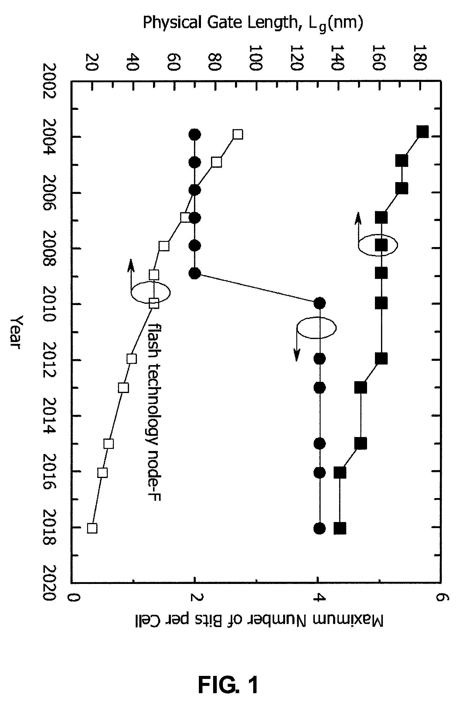
a flash memory and recess technology, applied in the field of flash memory devices, can solve the problems of large-scale integration, inability to reduce the scaling of flash memory devices having under 60 nm scale gate length, and increase the distribution of threshold voltage, so as to improve the fast erase characteristic, reduce the threshold voltage shift, and increase the channel controllability of the control electrode.

Active Publication Date: 2011-01-18
SEOUL NAT UNIV R&DB FOUND
View PDF12 Cites 0 Cited by
  • Summary
  • Abstract
  • Description
  • Claims
  • Application Information

AI Technical Summary

Benefits of technology

[0026]As described above, since multiple-bit flash memory device in accordance with the present invention has the recessed-channel structure and the triple-gate structure, it has both advantages of the existing double / triple-gate structure and the recessed-channel structure. Additional advantages together with these advantages are as follows:
[0027]As a first advantage, the existing bulk FinFET requires the active body width corresponding to ⅔ of the gate length, whereas the structure in accordance with the present invention has no problem even when making the body width equal to the 2-dimensional gate length, thereby provides the advantages intended in the present invention. The structure can also improve the fast erase characteristic through a body and write / erase characteristic through the increase of the channel controllability of the control electrode, and reduce the threshold voltage shift according to the substrate bias and the change of impurity density on the corner of the recessed-channel.
[0028]As a second advantage, since the channel is formed at the sidewalls as well as the surface of the recessed channel, the structure in accordance with the present invention can reduce the threshold voltage distribution of the flash memory device according to the high current driving capability and the increased effective channel area. The increase of the effective channel area is characterized by largely reducing the threshold voltage distribution in either case that uses a nitride film or high-k dielectrics as a storage node or nano-scale dots as a floating storage node.
[0029]As a third advantage, since the junction depth of a source / drain can be made deep, the structure in accordance with the present invention can greatly improve the erase speed through source, drain, or both the source and drain, as compared to the existing planer channel structure. In the structure, since the charge storage node is formed only on the vertical surface and sidewalls except near the floor of the recessed area, the charge storage node is separated each other centering around the floor of the recessed region. As a result, the redistribution of the charges stored through program can be reduced, and thereby improving the memory characteristics.
[0030]As a fourth advantage, since 1-bit can be stored in each source and drain respectively in the case that the material of the charge storage node is composed with a dielectric material or nano-scale dots, it is possible to realize 2-bit / cell. the structure in accordance with the present invention is characterized in that 2-bit / cell can be realized even when the material of storage node is conductive material in case that the storage electrode is completely separated as the form of a spacer.

Problems solved by technology

The down-scaling of the existing flash memory devices having under 60 nm scale gate length is in the verge of limitation.
If the size of a device having thick floating gate is reduced, the capacitance between devices is increased, thereby causing a cross-talk between cells, leading to increase the distribution of threshold voltage, and thus stumbling large scale integration.
Likewise, the existing devices have difficulties in down-scaling a device, improving read / write speeds, reducing cross-talk, and the like.
Thus, there is a disadvantage of degrading the current driving capability when the channel width becomes narrow.
The general feature of the recessed channel devices is that the channel controllability of control electrode is inferior to that of the planer channel devices.
The weakened channel controllability of a control electrode takes disadvantage of slowing write / erase characteristics through the control electrode.
his means that a silicon body is formed with narrower width than the minimum gate length, and thereby causing a problem in a fabrication process.
And it is easy that the charges stored in one side spreads to another side under a certain temperature, and thereby, easily losing the memory information.

Method used


Image

  • Flash memory device and fabricating method thereof comprising a body recess region
  • Flash memory device and fabricating method thereof comprising a body recess region
  • Flash memory device and fabricating method thereof comprising a body recess region

Examples


Embodiment Construction

[0047]Hereinafter, referring to appended drawings, the structures and operational principles for the embodiments of present invention are described in detail.

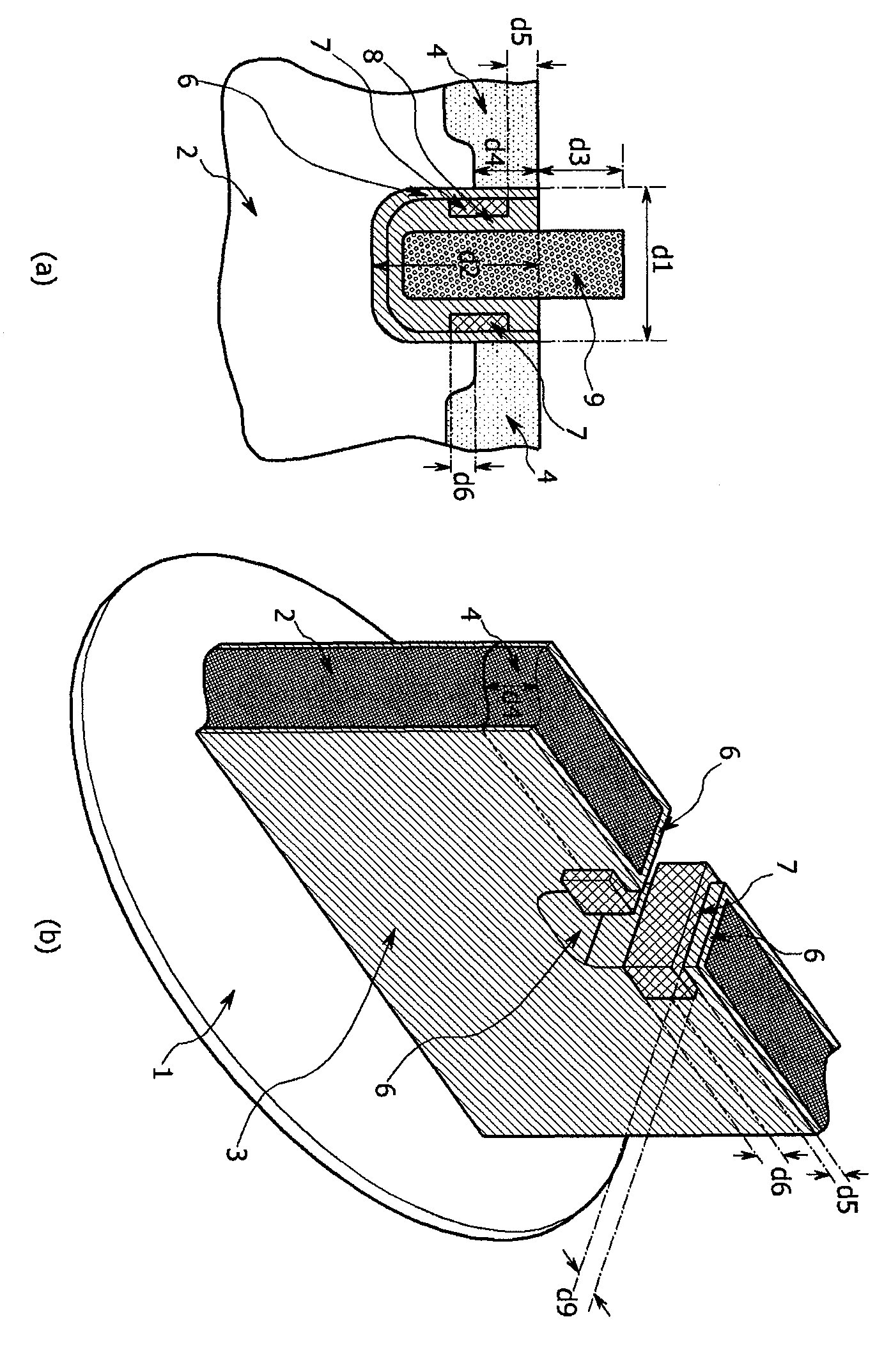
[0048]In the present invention, proposed a novel device structure settling the problems residing in the existing 2-bit / cell structures. FIG. 3(a) shows a cross-sectional view of the device proposed in the present invention, and FIG. 3(b) precisely shows the structure of the present invention, where the process is carried out up to the previous steps which the inter-electrode dielectric film is formed.

[0049]In FIG. 3(b), the field dielectric film region (5) of the truly existing region shows a recessed region and the principal structure around a wall-type body is also shown. In FIG. 3(b), the elliptic region (1) indicates a silicon wafer substrate. Basically, the principal parts of a device including storage nodes and channels are made in a recessed region. The width of the wall-type body is suitably formed in a range between 4 ...


PUM


Abstract

The present invention relates to a flash memory device and its fabrication method. The device comprises a structure for improving a scaling-down characteristic / performance and increasing memory capacity of the MOS-based flash memory device. A new device structure according to the present invention is based on a recessed channel capable of implementing highly-integrated / high-performance and 2-bit / cell. The proposed device suppresses the short channel effect, reduces the cell area, and enables 2-bit / cell by forming the charge storage node as a spacer inside the recessed channel. Moreover, if selectively removing the dielectric films around the recessed silicon surface, the sides as well as the surface of the recessed channel is exposed. A spacer can be used as a storage node, thereby improving the channel controllability of the control electrode and the on-off characteristic of a device. The proposed structure also resolves the threshold voltage problem and improves the write / erase speeds.

Description

TECHNICAL FIELD[0001]The present invention relates to a flash memory device and its fabrication method, in more detail, it relates to a novel device structure for improving a scaling-down characteristic / performance and increasing memory capacity of the MOS-based flash memory device.BACKGROUND ART[0002]With recent ever increasing demands for a flash memory in consumer electronics and portable electronic devices, flash memory is highly marketable, and thus the market is expected to exceed that of the existing DRAM around the year 2007. On the other hand, it is continuously required for memory devices to be highly integrated and fast in write / erase time.[0003]The down-scaling of the existing flash memory devices having under 60 nm scale gate length is in the verge of limitation. In order to increase the speed of write and read time in existing planer channel device structure, the capacitance between control gate and floating storage electrode should be increased. Also, the coupling rat...

Claims


Application Information

Patent Timeline
Patent Type & Authority Patents(United States)
IPC IPC(8): H01L29/788
CPCB82Y10/00H01L21/28273H01L21/28282H01L29/42332H01L29/42336H01L29/42348H01L29/42352H01L29/66825H01L29/66833H01L29/7881H01L29/7887H01L29/792H01L29/7923H01L29/785H01L29/40114H01L29/40117
Inventor LEE, JONG-HO
Owner SEOUL NAT UNIV R&DB FOUND
Why Eureka
Try Eureka