Waveguide forming apparatus, dielectric waveguide forming apparatus, pin structure, and high frequency circuit

a technology of dielectric waveguide and forming apparatus, which is applied in the direction of waveguides, leaky waveguide antennas, delay lines, etc., can solve the problems of large structure of high frequency circuit components, difficulty in realizing programmable center frequency and passband of wideband antennas or filters, and inability to realize software-defined radios that can be changed between multiple modes, etc., to achieve high versatility

Inactive Publication Date: 2011-01-25
KYOCERA CORP
View PDF18 Cites 26 Cited by
  • Summary
  • Abstract
  • Description
  • Claims
  • Application Information

AI Technical Summary

Benefits of technology

[0008]An object of the invention is to provide a waveguide forming apparatus, a dielectric waveguide forming apparatus, a pin structure, and a high frequency circuit that can optimize a circuit portion provided therein and have high versatility.

Problems solved by technology

However, it is difficult to realize programmable center frequency and passband of wideband antennas or filters that are required for this method.
With radio portions in which the passband is limited, a software-defined radio cannot be realized that can be changed between multiple modes.
With radio portions in which a plurality of types of high frequency circuit components are provided and selectively used, the structure of the high frequency circuit components becomes large and complex, which lacks versatility.
On the reception side, in a case where a plurality of high level signals are inputted to a desired band in a frequency converting portion, there is the problem that the dynamic range is lowered and a non-linear distortion of a mixer occurs.

Method used


Image

  • Waveguide forming apparatus, dielectric waveguide forming apparatus, pin structure, and high frequency circuit
  • Waveguide forming apparatus, dielectric waveguide forming apparatus, pin structure, and high frequency circuit
  • Waveguide forming apparatus, dielectric waveguide forming apparatus, pin structure, and high frequency circuit

Examples


Embodiment Construction

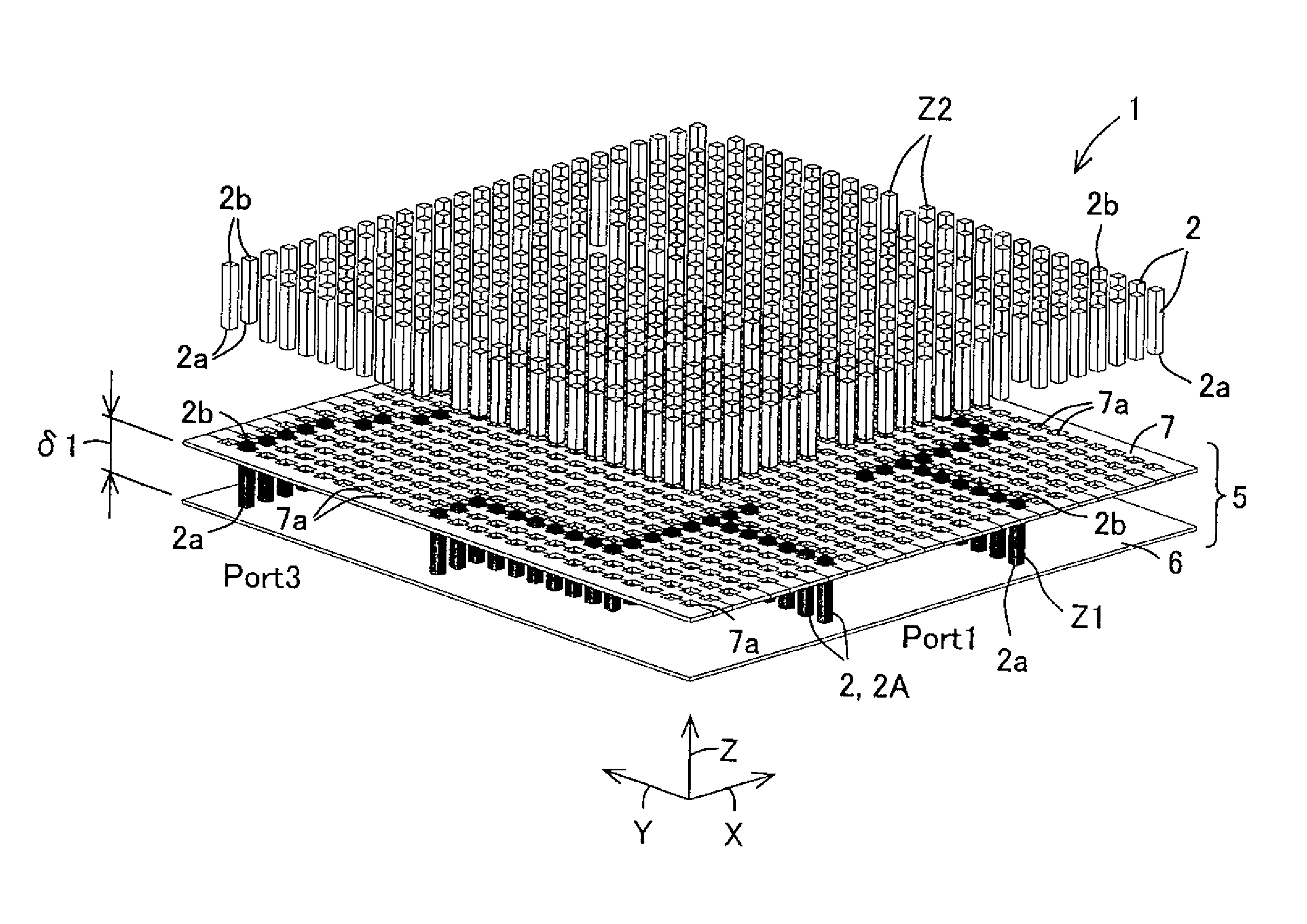
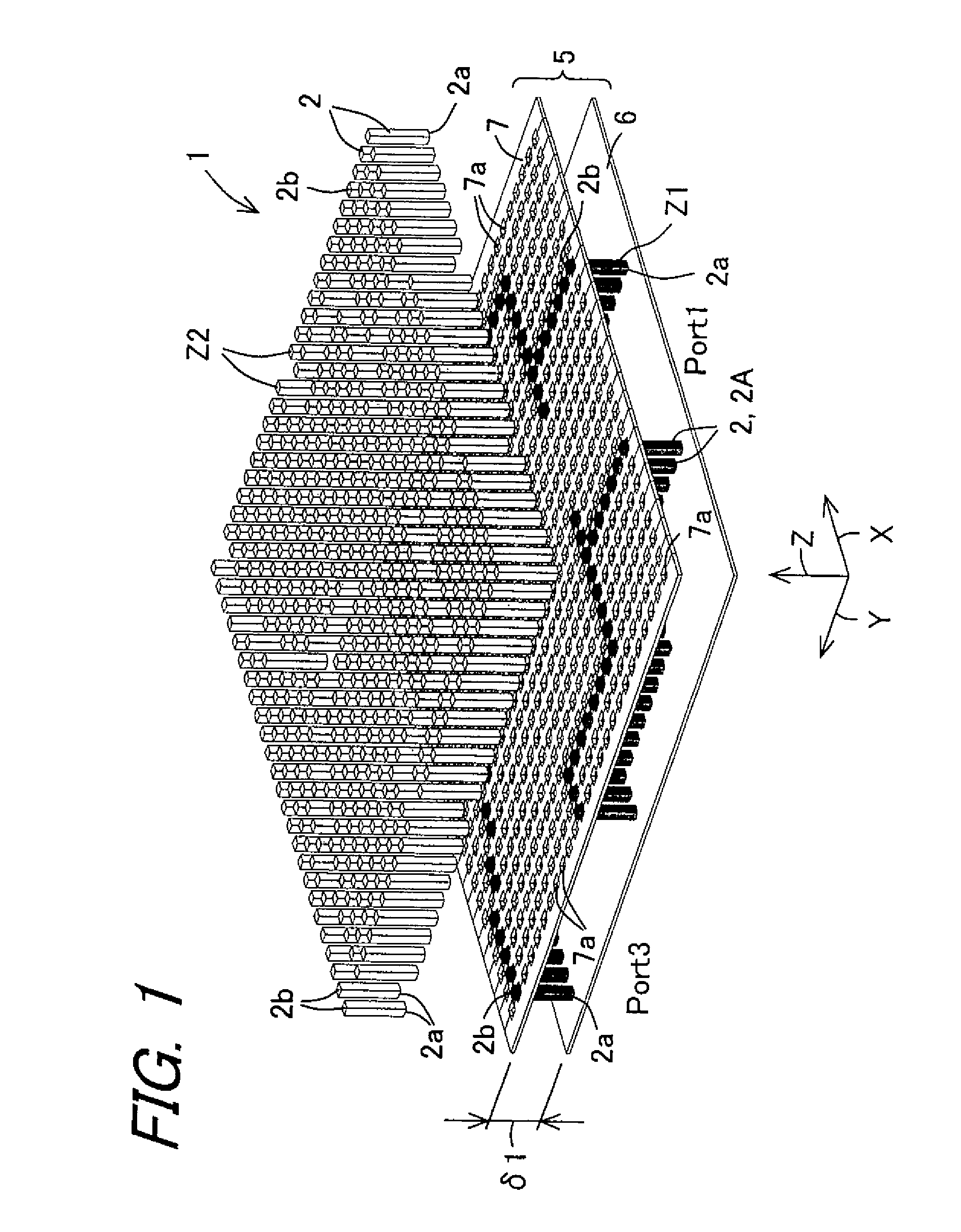
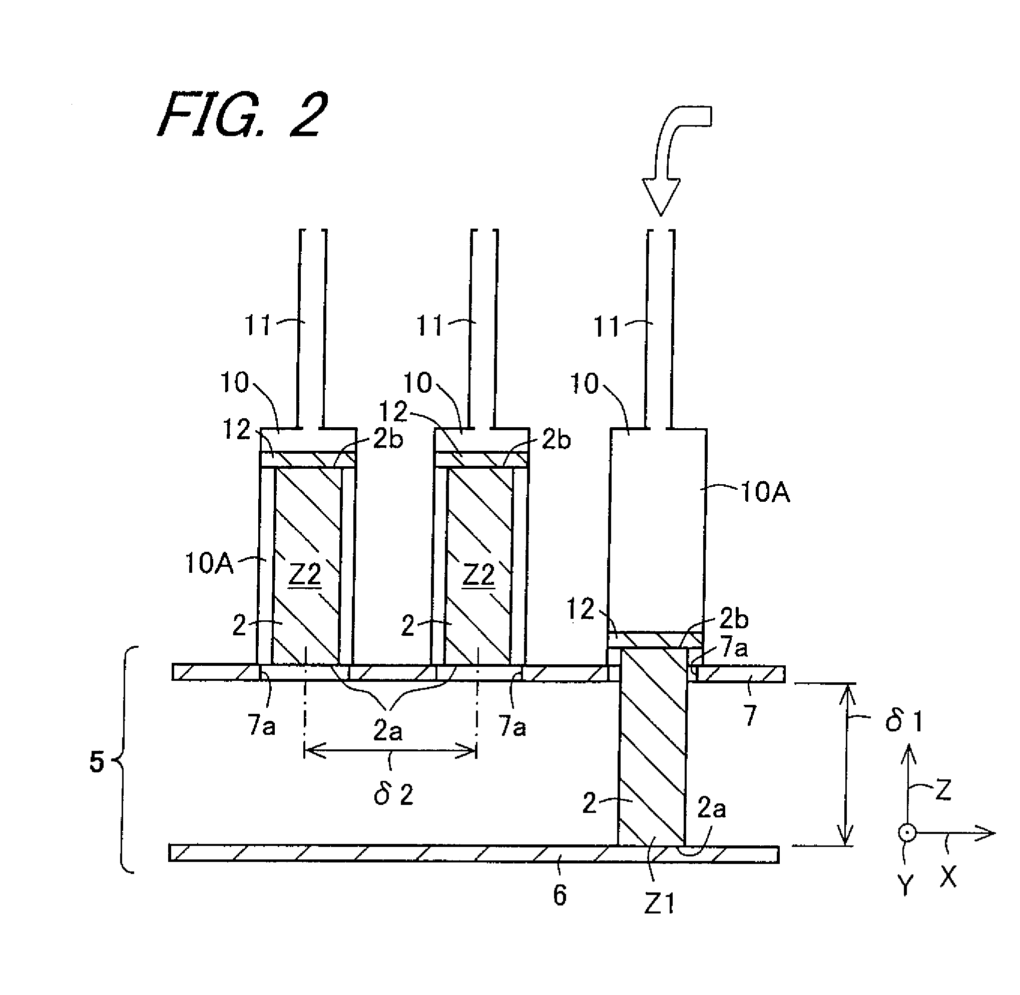
[0094]Now referring to the drawings, preferred embodiments of the invention are described below. In the description of the embodiments, a portion corresponding to that described in a foregoing embodiment may be denoted by the same reference numeral, and the description thereof may not be repeated. In a case where only a part of a configuration is described, the other portions of the configuration are similar to those previously described. In addition to a combination of portions specifically described in embodiments, a partial combination of the embodiments is also possible as long as the combination does not cause any problem. A variable high frequency circuit according to the embodiments is applicable to a plurality of high frequency circuit components such as antennas, waveguides, power dividers, couplers, and filter circuits. In the description below, a method for controlling a variable high frequency circuit, and a pin structure of control pins are also described.

[0095]FIG. 1 i...


PUM


Abstract

There are provided a waveguide forming apparatus, a dielectric waveguide forming apparatus, a pin structure and a high frequency circuit that can optimize a circuit portion provided therein and have high versatility. A waveguide is formed by allowing first and second conductive layers (6, 7) to cooperate with a plurality of control pins (2). A variable high frequency circuit forming portion is freely and simply changed by displacing each control pin (2) between a down-status indicated by Z1 and an up-status indicated by Z2.

Description

CROSS-REFERENCE TO THE RELATED APPLICATIONS[0001]This application is a national stage of international application No. PCT / JP2007 / 054593 filed Mar. 8, 2007, which also claims the benefit of priority under 35 U.S.C. §119 to Japanese Patent Application No. 2006-064482 filed Mar. 9, 2006, Japanese Patent Application No. 2006-096034 filed Mar. 30, 2006 and Japanese Patent Application No. 2006-209312 filed Jul. 31, 2006, the entire contents of all of which are incorporated herein by reference.TECHNICAL FIELD[0002]The present invention relates to a waveguide forming apparatus, a dielectric waveguide forming apparatus, a pin structure, and a high frequency circuit, and, for example, relates to techniques preferably applied to a high frequency circuit component such as an antenna, a filter, or a coupler circuit.BACKGROUND ART[0003]Recently, research on software-defined radios is being intensively conducted (see Japanese Patent Nos. 3686736, 3439973, and 3517097, Japanese Unexamined Patent P...

Claims


Application Information

Patent Timeline
Patent Type & Authority Patents(United States)
IPC IPC(8): H01P3/16H01P5/04
CPCH01P1/122H01P3/12H01P3/121H01P5/04H01Q13/22
Inventor UCHIMURA, HIROSHI
Owner KYOCERA CORP
Why Eureka
Try Eureka