Developing method and method for fabricating semiconductor device using the developing method

a technology of developing method and developing method, which is applied in the direction of photomechanical equipment, instruments, photosensitive material processing, etc., can solve the problem of large pattern size variation, and achieve the effect of preventing pattern size variation

Active Publication Date: 2011-02-08
PANASONIC SEMICON SOLUTIONS CO LTD
View PDF7 Cites 0 Cited by
  • Summary
  • Abstract
  • Description
  • Claims
  • Application Information

AI Technical Summary

Benefits of technology

[0009]It is therefore an object of the present invention to prevent a variation in pattern size (opening size) from occurring even when regions having different opening ratios are provided in a multi-stage developing method for a resist pattern.
[0010]To achieve the object, in a developing method according to the present invention, the rotation speed of a wafer in a developer removing step of removing a developer and a resist dissolved in the developer before a rinsing step is lower than that in the rinsing step or the rotation time of the wafer in removing a developer and a resist dissolved in the developer is shorter than that in the rinsing step.
[0011]With this method, the difference in concentration of developers due to a density variation between patterns in a wafer plane is reduced, so that the opening sizes in the wafer plane between resist patterns become uniform.
[0013]In a conventional method, since the rotation speed is substantially equal to that in the rinsing step, a developer which is supplied onto a first region having a relatively low opening ratio and in which a resist is dissolved is flung off from an opening pattern. In addition, a larger amount of a developer which is supplied onto a second region having a relatively high opening ratio and in which the resist is dissolved flows into portions as the distance from the first region decreases. Accordingly, the degree of freshness (i.e., concentration) of a developer remaining in the opening pattern in the first region having a relatively low opening ratio varies depending on the location. However, according to the present invention, the rotation speed of the substrate in the developer removing step is one half or less of that in the rinsing step, so that the developer is not flung off from the opening pattern in the first region having a relatively low opening ratio. Accordingly, the degree of freshness of the developer remaining in the opening pattern in the first region does not vary depending on the location, so that a variation in pattern size among opening patterns is prevented.
[0017]In the third developing method, the rotation time of the substrate in the first developer removing step is shorter than that in the rinsing step, so that a developer is not flung off from the opening pattern in a region having a relatively low opening ratio. Accordingly, the degree of freshness of the developer remaining in the opening pattern in the region having a relatively low opening ratio does not vary depending on the location, so that a variation in pattern size among opening patterns is prevented.

Problems solved by technology

Accordingly, the method is susceptible to the influence of density variation between patterns, resulting in a large variation in pattern size (which will be described later in detail).

Method used


Image

  • Developing method and method for fabricating semiconductor device using the developing method
  • Developing method and method for fabricating semiconductor device using the developing method
  • Developing method and method for fabricating semiconductor device using the developing method

Examples


embodiment 1

[0043]A first embodiment of the present invention will be described with reference to the drawings.

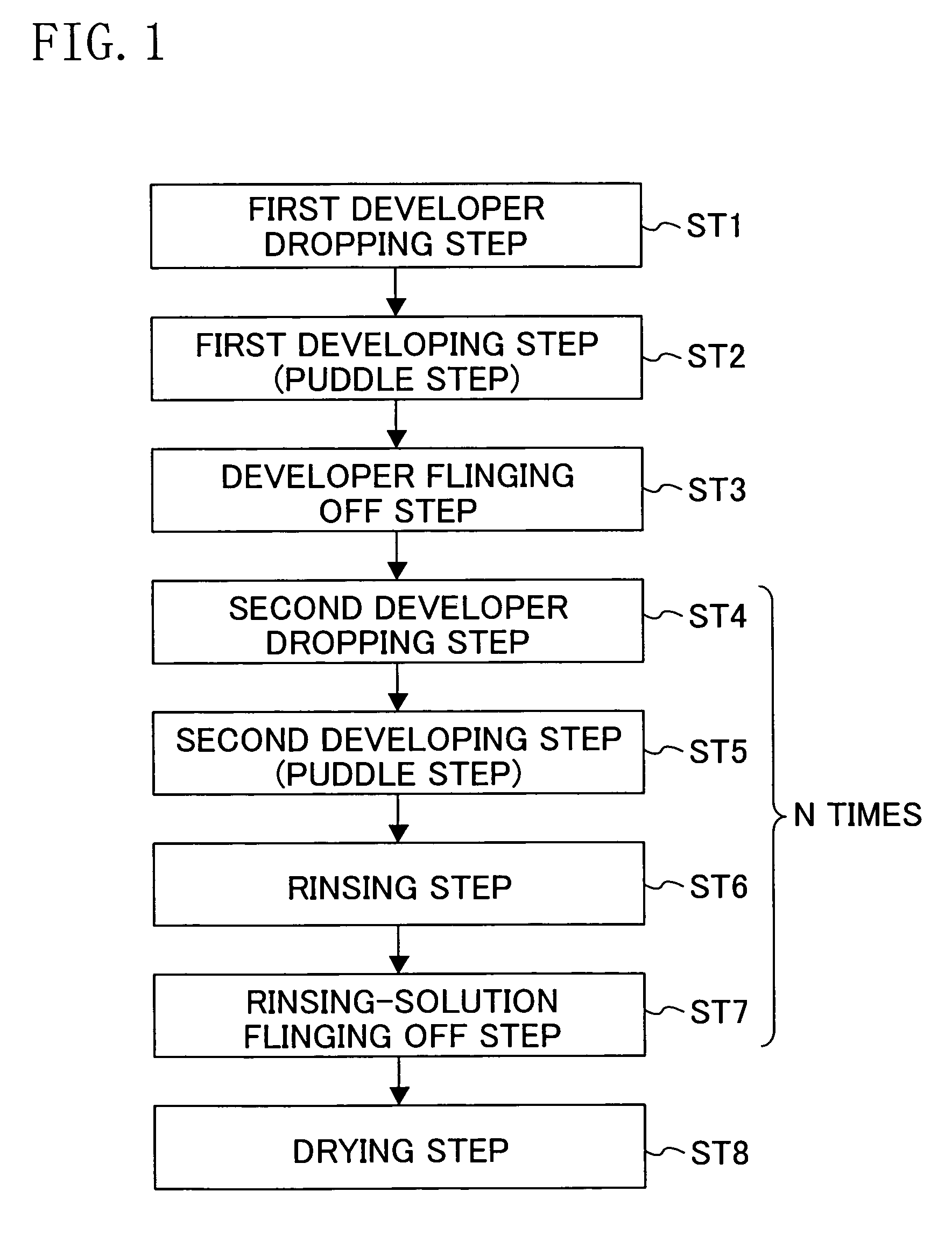
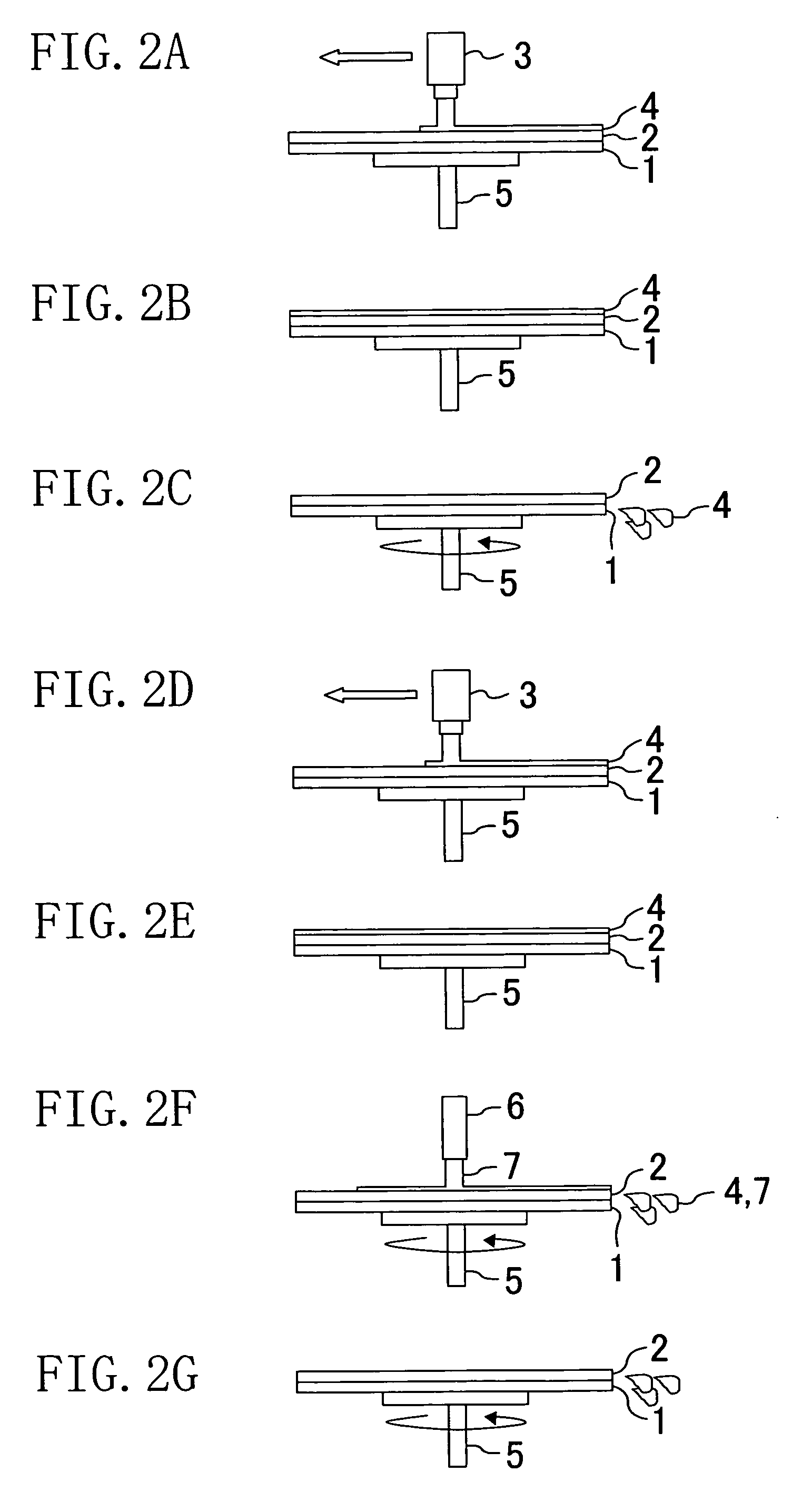
[0044]FIG. 1 shows a flow of processes in a method for developing a resist according to the first embodiment. FIGS. 2A through 2G are side views schematically showing a method for developing a resist according to the process flow shown in FIG. 1.

[0045]In the first embodiment, so-called multi-stage development is performed. Specifically, a developer is supplied onto a resist film, and then a wafer is rotated without addition of a rinsing solution (pure water) so as to fling off and remove the developer. Thereafter, a developer is supplied onto the resist film again to perform second development. When necessary, third development is performed.

[0046]First, though not shown, the principal surface of the wafer having a diameter of, for example, 20.3 cm (i.e., 8 inches) and made of silicon (Si) is coated with a resist film by a spin coating process.

[0047]Next, a design pattern including a pa...

embodiment 2

[0075]Hereinafter, a developing method for a resist according to a second embodiment of the present invention will be described.

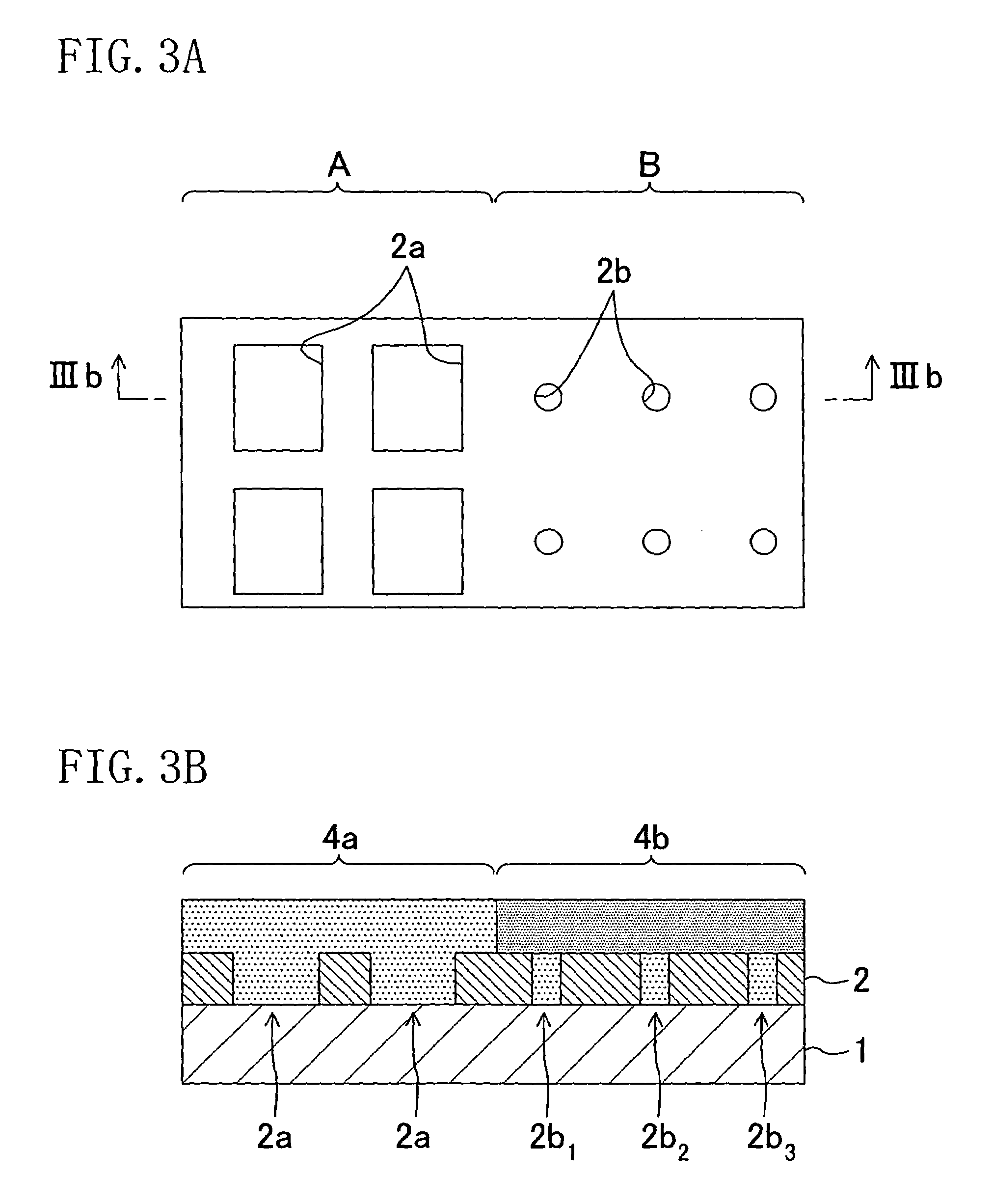
[0076]The second embodiment is also directed to a resist film 2 shown in FIG. 3A and adjacent design patterns having different opening ratios are exposed on the resist film 2.

[0077]The second embodiment is different from the first embodiment in that the rotation speed of the wafer in the developer flinging off step ST3 is set at a half or less of that in the rinsing step in the first embodiment, whereas the rotation speed in a developer flinging off step ST3 is equal to that in a rinsing step but the rotation time is shorter than that in the rinsing step in the second embodiment.

[0078]Specifically, in the second embodiment, in the developer flinging off step ST3, the rotation speed and time are set not to dry a resist film 2 on a wafer 1 and the fling-off time of a developer 4 is set such that the rotation speed is 3000 rpm and the rotation time is set at o...

embodiment 3

[0083]Hereinafter, a third embodiment of the present invention will be described with reference to the drawings.

[0084]FIGS. 8A and 8B and FIG. 9 illustrate cross-sectional structures of respective process steps of a method for fabricating a semiconductor device according to the third embodiment using the developing method for a resist of the first or second embodiment.

[0085]First, as shown in FIG. 8A, a plurality of transistors (field effect transistors) 31 are formed in a wafer (substrate) 30 made of silicon and are isolated from each other by a trench isolation film 32.

[0086]A first insulating film 33A made of, for example, silicon oxide and having a planarized upper surface is formed on the wafer 30 to cover the transistors 31. A plurality of first contact plugs 34A are formed in the first insulating film 33A and electrically connected to source / drain regions of the first transistors 31. A plurality of first interconnections 35A containing an aluminum alloy as a main component ar...


PUM

PropertyMeasurementUnit
distanceaaaaaaaaaa
diameteraaaaaaaaaa
diameteraaaaaaaaaa

Abstract

In a developing method, a developer is supplied onto a resist film provided on a substrate, made of a resist and having an upper surface on which design patterns having different mask opening ratios are exposed and a development reaction is caused to proceed on the resist film with the supplied developer. After the development, the substrate is rotated so that the developer and the resist dissolved in the developer are removed. Then, a rinsing solution is supplied onto the resist film subjected to development and the substrate is rotated, thereby washing out the developer and the resist dissolved in the developer. The rotation speed of the substrate in removing the developer is a half or less of the rotation speed of the substrate in the rinsing step of washing out the resist.

Description

CROSS-REFERENCE TO RELATED APPLICATION[0001]The disclosure of Japanese Patent Application No. 2006-133987 filed in Japan on May 12, 2006 including specification, drawings and claims is incorporated herein by reference in its entirety.BACKGROUND OF THE INVENTION[0002]The present invention relates to a method for developing a resist film for use in photolithography and a method for fabricating a semiconductor device using the developing method.[0003]A photolithography process in conventional semiconductor fabrication includes: a process of applying a resist onto the principal surface of a semiconductor substrate (i.e., a wafer); an exposure process of burning a design pattern on the resist film; and a developing process of eluting a region exposed to light or a region not exposed to light so as to form a resist pattern.[0004]A developing process generally uses a developing method in which a developer discharging nozzle supplies a developer from a given position onto the entire surface...

Claims


Application Information

Patent Timeline
Patent Type & Authority Patents(United States)
IPC IPC(8): G03F7/32
CPCG03F7/3021B05C11/10G03F7/3057H01L21/02057H01L21/6704H01L21/6715
Inventor KITAHARA, HIDEKAZUNODA, KENJIASAHI, KENICHIUJIMARU, NAOHIKOFUKUMOTO, HIROFUMI
Owner PANASONIC SEMICON SOLUTIONS CO LTD
Why Eureka
Try Eureka