Exposure apparatus and method of manufacturing device

a technology of manufacturing device and exposure apparatus, which is applied in the direction of photomechanical treatment, printing, instruments, etc., can solve the problems of difficult to mechanically inhibit a change in the shape of the bar mirror, the bar mirror may gradually or abruptly deform, and the entire surface of the bar mirror processing is difficul

Inactive Publication Date: 2011-02-08
CANON KK
View PDF5 Cites 414 Cited by
  • Summary
  • Abstract
  • Description
  • Claims
  • Application Information

AI Technical Summary

Benefits of technology

[0030]The present invention provides an exposure apparatus which can measure an error in the optical axis direction of a projection optical system, which is attributed to the driving of a substrate stage, without stopping an exposure process.
[0032]According to the present invention, it is possible to provide an exposure apparatus which can measure an error in the optical axis direction of a projection optical system, which is attributed to the driving of a substrate stage, without stopping an exposure process. This makes it possible to simultaneously optimize the accuracy and productivity of the exposure apparatus.

Problems solved by technology

Although a positioning accuracy in the Z direction on the nanometer order is required as described above, it is technically difficult to process the entire surfaces of bar mirrors with an accuracy on the nanometer order and assemble the thus processed mirrors.
In this technique, however, a plurality of focus sensors are used to eliminate the influence of the wafer surface shape, and measure an error in the moving plane of the stage alone.
Nevertheless, the bar mirror may gradually or abruptly deform due to various factors.
In other words, it is very difficult to mechanically inhibit a change in the shape of the bar mirror with an accuracy on the nanometer order.
Even if the shape of the Z bar mirror can be corrected with high accuracy by the method described in Japanese Patent Laid-Open No. 2001-015422, the positioning accuracy in the Z direction often degrades gradually or abruptly.
Unfortunately, even in this case, the productivity of the exposure apparatus lowers because of the necessity of measurement while the exposure process is stopped.
The rate of deformation of the bar mirror varies depending on the performances of individual exposure apparatuses, so it is hard to know an appropriate measurement timing.
If the measurement is performed at too long an interval, the amount of deformation of the bar mirror becomes too large, and this may produce defective products.
Conversely, if the measurement is performed too frequently, the operating rate of the exposure apparatus lowers, resulting in degradation in the productivity.
Furthermore, in both cases, the above-mentioned method cannot cope with a situation in which the bar mirror has deformed abruptly.

Method used


Image

  • Exposure apparatus and method of manufacturing device
  • Exposure apparatus and method of manufacturing device
  • Exposure apparatus and method of manufacturing device

Examples


Embodiment Construction

[0049]Embodiments of a single-stage exposure apparatus and twin-stage exposure apparatus according to the present invention will be individually explained below.

[0050][Twin-Stage Exposure Apparatus]

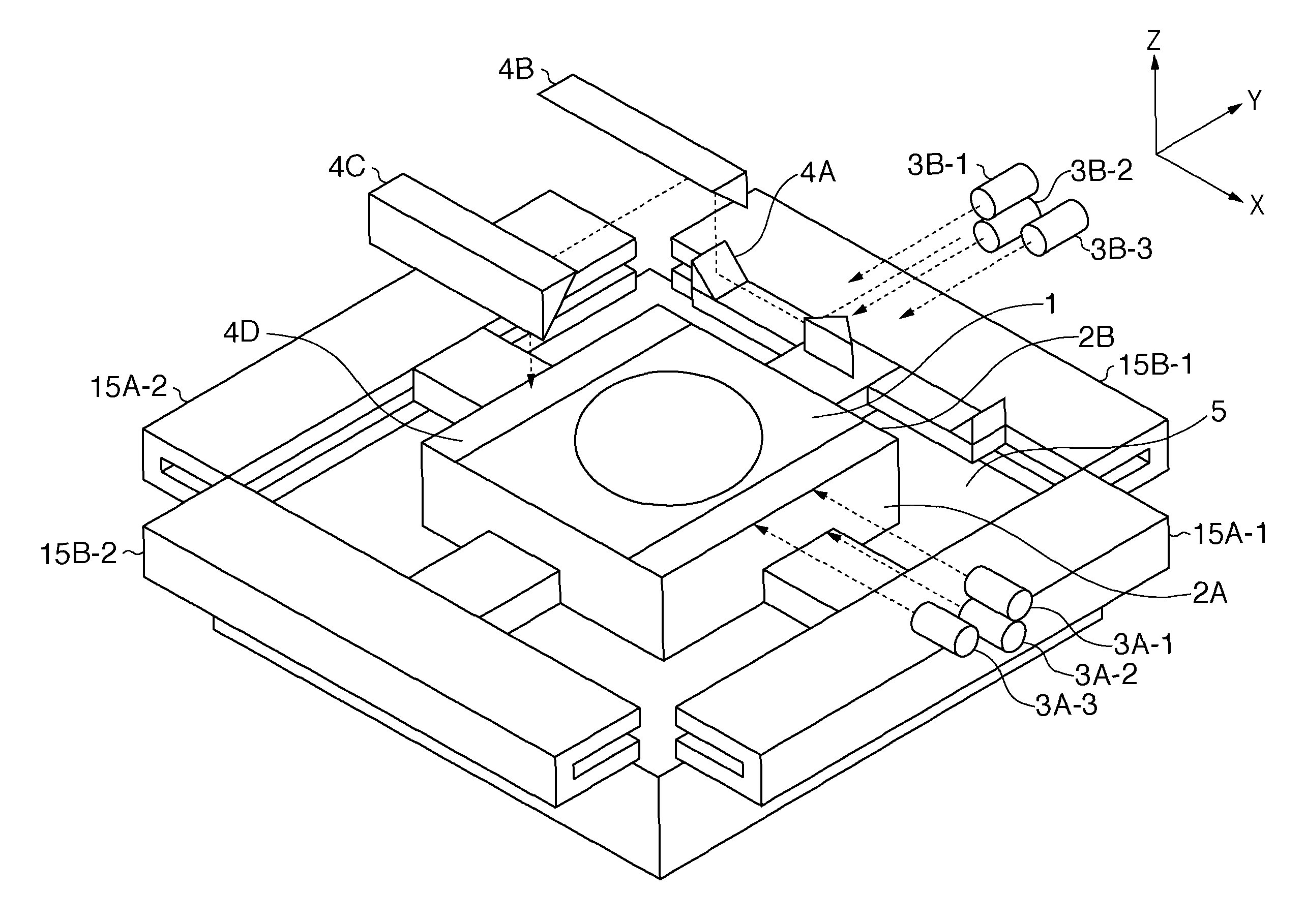
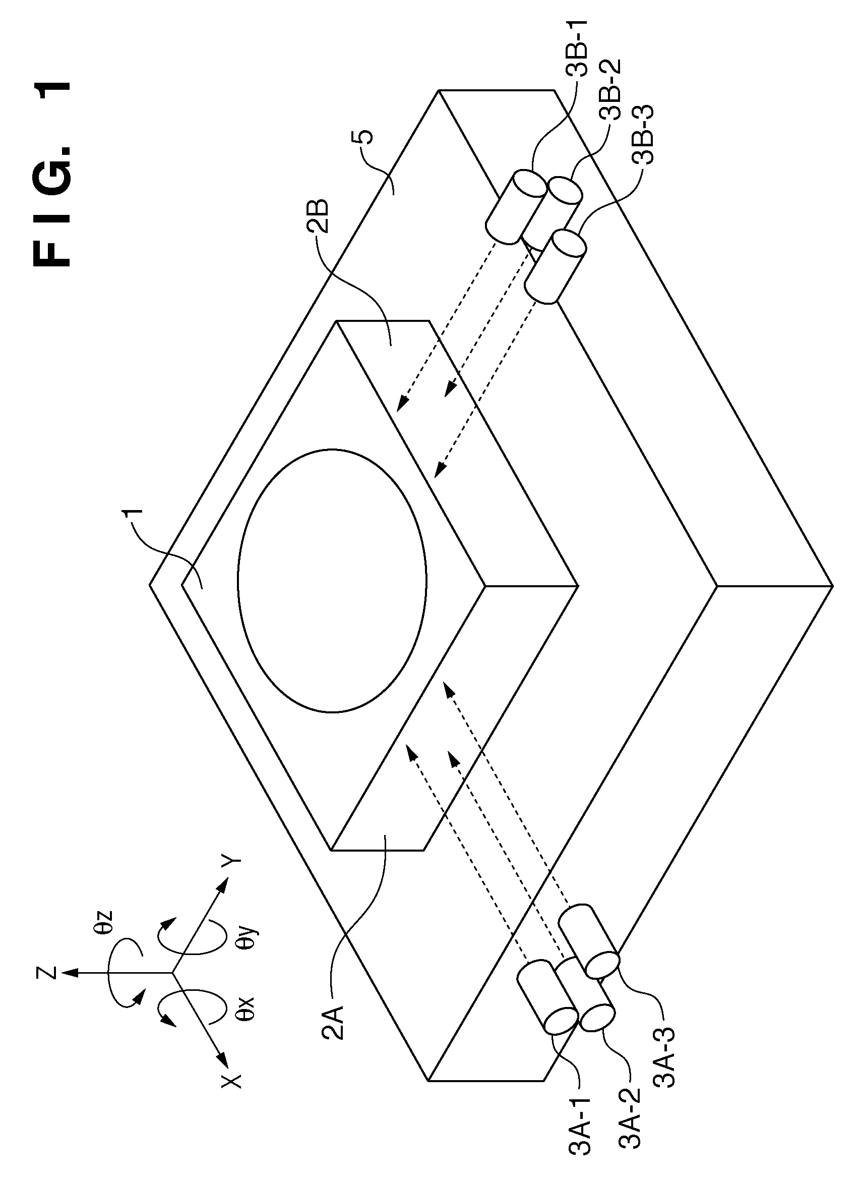
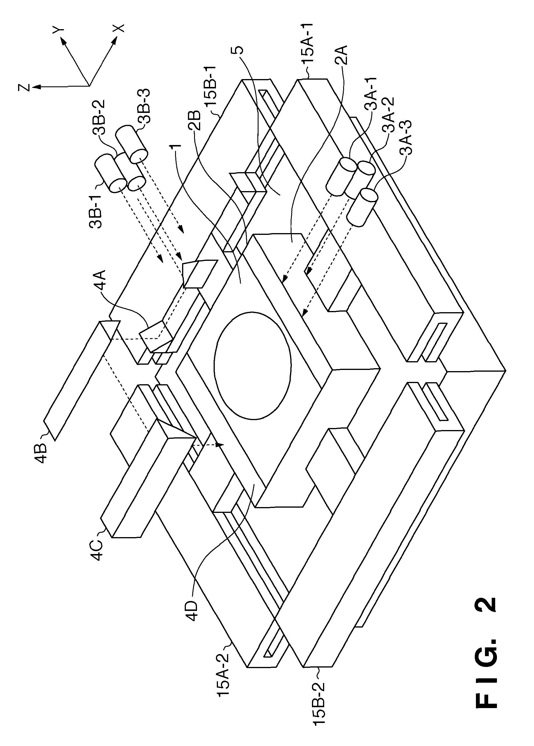
[0051]A twin-stage exposure apparatus includes an exposure region, a measurement region, and a plurality of substrate stages which can move in the exposure region and the measurement region. The exposure apparatus exposes the substrate, which is measured in the measurement region, in the exposure region while positioning the substrate in accordance with the measurement result.

[0052]A twin-stage exposure apparatus measures the surface position (level position) of a substrate (wafer) in the optical axis direction of a projection optical system at the OAS position in the measurement region before an exposure process, as shown in FIG. 7. A plurality of measurement points 7-1 to 7-5 of second measurement devices (focus sensors) which measure the substrate level position (focus position) align ...


PUM


Abstract

An exposure apparatus includes a first measurement device, a second measurement device, and a controller. The first measurement device measures the position of a substrate stage in the optical axis direction when the substrate stage is scanned in the first direction. The second measurement device measures the surface positions of the substrate in the optical axis direction at a plurality of measurement points on one straight line extending in the second direction on the substrate. The controller controls the second measurement device to measure at least one identical region on the substrate at different measurement points of the plurality of measurement points both before and after the substrate stage moves in steps in the second direction, and calculates a measurement error of the first measurement device attributed to the driving of the substrate stage in the second direction based on the measurement result obtained by the second measurement device.

Description

BACKGROUND OF THE INVENTION[0001]1. Field of the Invention[0002]The present invention relates to an exposure apparatus and a method of manufacturing a device.[0003]2. Description of the Related Art[0004]The current mainstream semiconductor exposure apparatus is an exposure apparatus of the step & repeat scheme called a stepper. The stepper reduces, at a predetermined ratio, the information of light having passed through an original on which a pattern is drawn, and exposes a photosensitive agent applied on a substrate to light to transfer the pattern of the original onto the substrate, while the substrate is positioned to stand still at a predetermined position. The stepper repeats this series of exposure operations over the entire substrate surface by driving a substrate stage which holds the substrate step by step. A substrate, an original, and a photosensitive agent are commonly referred to as a wafer, a reticle, and a resist, respectively.[0005]In contrast to a stepper which perf...

Claims


Application Information

Patent Timeline
Patent Type & Authority Patents(United States)
IPC IPC(8): G03B27/68G03B27/42
CPCG03F7/70508G03F7/70525G03F7/70725G03F7/70775G03F7/70358H01L21/67259
Inventor HATTORI, TADASHI
Owner CANON KK
Why Eureka
Try Eureka