MRAM with cross-tie magnetization configuration

a magnetization configuration and cross-tie technology, applied in the field of magnetoresistive memory elements, can solve the problems of higher bit and word currents, errors may occur in half-select cells, etc., and achieve the effect of reducing half-select errors, raising the switching energy barrier of the free layer, and not increasing programming currents

Active Publication Date: 2011-02-08
TAIWAN SEMICON MFG CO LTD
View PDF8 Cites 5 Cited by
  • Summary
  • Abstract
  • Description
  • Claims
  • Application Information

AI Technical Summary

Benefits of technology

[0016]Another object of at least one embodiment of the present invention has been to increase the value of the easy axis field when the hard axis field is close to zero.
[0017]Still another object of at least one embodiment of the present invention has been to eliminate said half-select problem without increasing programming currents.
[0018]A further object of at least one embodiment of the present invention has been to eliminate the half select problem without using a segmented-array architecture.
[0019]These objects have been achieved by giving the free layer a shape that approximates an X so that, when the free layer switches, the magnetization in the arms of the X guides the magnetization in the central section (the X's intersection area) so that it rotates towards the hard axis in two opposing directions. This raises the free layer's switching energy barrier, thereby reducing half-select errors.
[0020]The invention discloses the detailed design rules for forming such a free layer and presents data confirming that, relative to an elliptically shaped free layer, the X-shape results in about a 5× increase of the easy axis field at zero hard axis field. Even relative to the C-shape, there is about a 3× increase. This improvement effectively solves the half-select problem.

Problems solved by technology

Although these fields are smaller than the combined field at the selected cell, these cells can still be accidentally programmed, thereby causing an error.
It follows from the above discussion that the values of both bit and word currents have to be carefully set—too low and the selected cell cannot be programmed reliably, too high and errors may occur in half-selected cells.
However such an approach demands higher bit and word currents which is undesirable in high density applications.

Method used


Image

  • MRAM with cross-tie magnetization configuration
  • MRAM with cross-tie magnetization configuration
  • MRAM with cross-tie magnetization configuration

Examples


Embodiment Construction

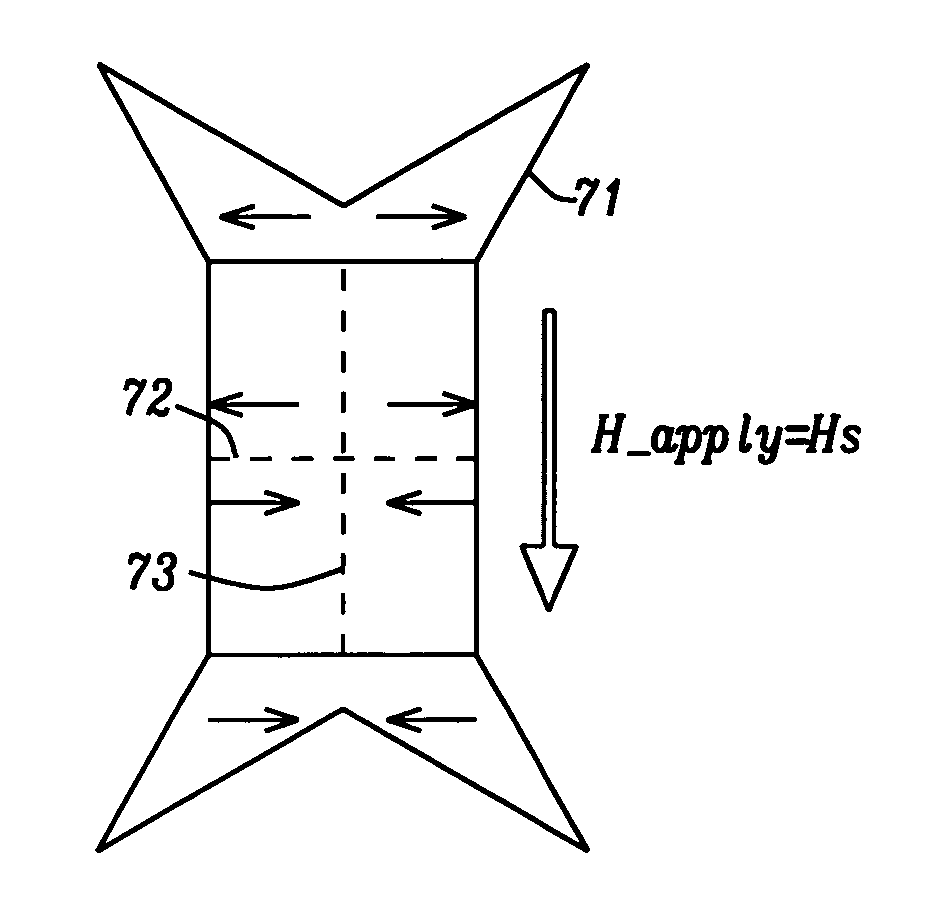
[0031]The invention discloses a new design for the shape of the free layer in a magneto-resistive device that is part of an MRAM. This design confines the quiescent free layer magnetization in a new state, the cross-tie (x-tie) state, as schematically illustrated by the example shown in FIG. 7a. The key feature of this design is that there are branches 71 that extend away from the top and / or bottom corners of the cell in the same general direction as a diagonal while also bending somewhat towards the hard axis direction. This type of cell shape forces the quiescent magnetization states of the free layer into a cross-tie (x-tie) configuration, as indicated by the arrows in FIG. 7a.

[0032]During switching, the magnetization in the branches serves to guide the central magnetization to rotate toward the hard axis, but in opposite directions (see FIG. 7b), creating, at switching, a pair of transient domain walls of opposite sign to each other (simplistically illustrated in FIG. 7c). Thes...


PUM


Abstract

The incidence of half-select errors during MRAM programming has been significantly reduced by giving the free layer a shape that approximates an X so that, when the free layer switches, the magnetization in the arms of the X guides the magnetization in the central section (the X's intersection area) causing it to rotate towards the hard axis in two opposing directions. This raises the free layer's switching energy barrier, thereby reducing half-select errors.

Description

FIELD OF THE INVENTION[0001]The invention relates to the general field of magneto-resistive memory elements with particular reference the free layer and, more particularly, to its shape.BACKGROUND OF THE INVENTION[0002]Referring now to FIG. 1a, a magnetic tunneling junction (MTJ) or a giant magneto-resistance (GMR) / Spin Valve (SV) has two ferromagnetic layers, 11 and 12, separated by non-magnetic layer 13 which is a tunneling layer in a MTJ or a metal spacer layer in a GMR / SV. This basic structure has been widely studied for use as a storage element in a magnetic random access memory (MRAM). Usually, one of the ferromagnetic layers (11) has a fixed direction of magnetization (pinned reference layer), while the other layer (12) is free to switch its magnetization direction, and is called the free layer.[0003]For MRAM applications, the MTJ or GMR stack is usually formed so as to provide shape anisotropy. This shape anisotropy comes about when the stack's shape ceases to be circular, t...

Claims


Application Information

Patent Timeline
Patent Type & Authority Patents(United States)
IPC IPC(8): G11C11/00
CPCB82Y25/00G11C11/16H01F10/325H01F10/3254G11C11/161G11C11/1675Y10S977/935
Inventor MIN, TAIHEIM, DAVID
Owner TAIWAN SEMICON MFG CO LTD
Why Eureka
Try Eureka