Method of manufacturing semiconductor laser using end-face-processing jig

a technology of end-face processing and semiconductor laser, which is applied in the direction of semiconductor lasers, liquid surface applicators, coatings, etc., can solve the problems of deteriorating the reliability of semiconductor lasers, and achieve the effect of preventing optical damage and deterioration of semiconductor lasers

Inactive Publication Date: 2011-02-22
MITSUBISHI ELECTRIC CORP
View PDF6 Cites 1 Cited by
  • Summary
  • Abstract
  • Description
  • Claims
  • Application Information

AI Technical Summary

Benefits of technology

[0007]It is an object of the present invention to provide an end-face-processing jig that allows the formation of a reflectance control film on an end face of a semiconductor laser body while preventing possible optical damage and deterioration of a semiconductor laser, and to provide a method of manufacturing a semiconductor laser employing such an end-face-processing jig.
[0009]The end-face-processing jig described above prevents a metal from being taken in a reflectance control film, thus preventing the absorption of light caused by a metal taken in the reflectance control film. This allows the formation of a reflectance control film on the end face of a semiconductor laser body while preventing possible degradation due to catastrophic optical damage (COD) of the semiconductor laser.
[0011]The above-described method of manufacturing a semiconductor laser prevents a metal from being taken in the reflectance control film formed on an end face of a semiconductor laser body, thus preventing the absorption of light caused by a metal taken in the reflectance control film. This prevents possible degradation due to COD of a semiconductor laser and produces a high-reliability semiconductor laser.
[0013]Unlike in the case where the window part and the spacers are made of a metal, the above-described method of manufacturing a semiconductor laser can prevent a metal from being taken in the reflectance control film, thus preventing the absorption of light caused by a metal taken in the reflectance control film even if the materials for the window part and the spacers are released by etching. In particular, the above-described method of manufacturing a semiconductor laser more reliably prevents a metal from being taken in the reflectance control film. This allows more reliable prevention of possible degradation due to COD of a semiconductor laser and produces a high-reliability semiconductor laser.

Problems solved by technology

In these techniques, however, particles of a material for a reflectance control film have energy, and having that energy they will collide with a jig for fixing semiconductor laser bars and spacers or with the spacers.
If lasing occurs with a metal taken in the reflectance control film, the metal would absorb light and undesirably cause degradation due to catastrophic optical damage (COD), thereby deteriorating the reliability of a semiconductor laser.

Method used


Image

  • Method of manufacturing semiconductor laser using end-face-processing jig
  • Method of manufacturing semiconductor laser using end-face-processing jig
  • Method of manufacturing semiconductor laser using end-face-processing jig

Examples


first preferred embodiment

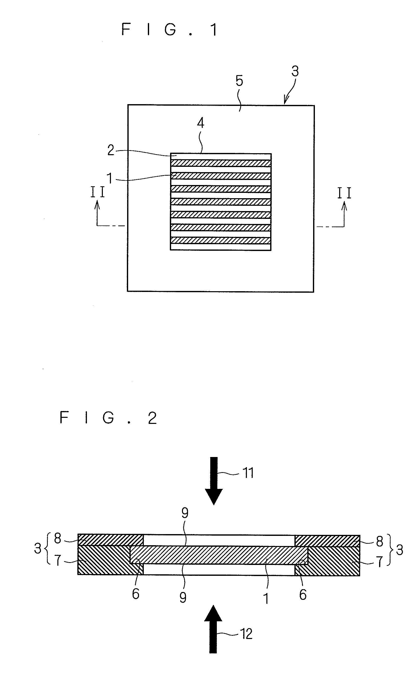
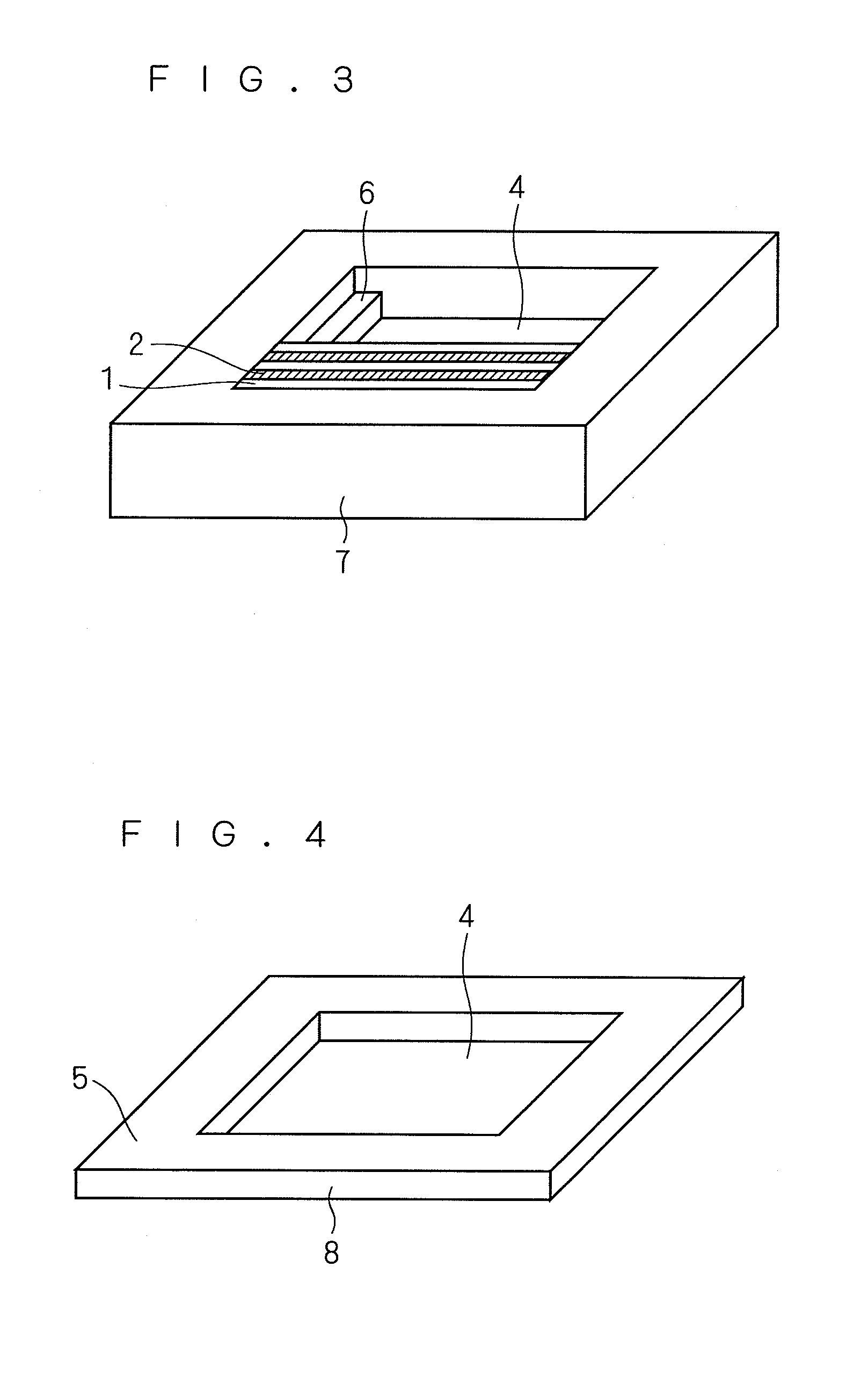
[0025]FIG. 1 is a plan view of a semiconductor laser's end-face-processing jig 3 according to a first preferred embodiment of the invention. FIG. 2 is a cross-sectional view taken along line II-II in FIG. 1. FIG. 3 is a simplified perspective view of a holding jig 7. FIG. 4 is a simplified perspective view of a fixing jig 8. Referring to FIG. 1, semiconductor laser bars 1 obtained by cleaving a wafer 15 into bars, which will be described later with reference to FIG. 5, and spacers 2 are arranged alternately and fixed to a semiconductor laser's end-face-processing jig (hereinafter referred to simply as an “end-face-processing jig) 3. In other words, a plurality of semiconductor laser bars 1 that are arranged with each spacer 2 interposed between each adjacent two of them and that are fixed to the end-face-processing jig 3 are illustrated in FIG. 1.

[0026]Each semiconductor laser bar 1 is, as will be described later with reference to FIG. 6, formed of a plurality of semiconductor laser...

second preferred embodiment

[0043]Next described is an end-face-processing jig and a method of manufacturing a semiconductor laser using the end-face-processing jig according to a second preferred embodiment of the invention. The steps in the production of a semiconductor laser bar according to the present preferred embodiment are identical to those previously described in the first preferred embodiment, so that corresponding parts are designated by the same reference numerals and redundant descriptions of the common parts to those in the first preferred embodiment are omitted herein.

[0044]Although the first preferred embodiment has described the end-face-processing jig 3 made of either an oxide or a nitride, oxide and nitride are difficult to process as compared to metal and cause an increase in manufacturing cost. Thus, the holding jig 7 having in particular the spot facing part 6 should desirably be made of a metal such as stainless used steel (SUS).

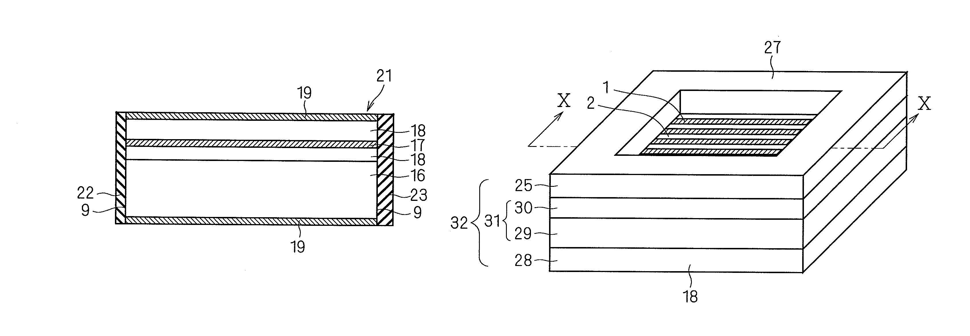
[0045]An end-face-processing jig 32 according to the prese...

third preferred embodiment

[0051]Next described is an end-face-processing jig and a method of manufacturing a semiconductor laser using the end-face-processing jig according to a third preferred embodiment of the invention. Both the steps in the production of a semiconductor laser bar and the end-face-processing jig according to the present preferred embodiment are identical to those previously described in the first preferred embodiment, so that corresponding parts are designated by the same reference numerals and redundant descriptions of the common parts to those in the first preferred embodiment are omitted herein.

[0052]In forming a reflectance control film, the material for the reflectance control films 22 and 23 is deposited not only on the end-face-processing jig 3 but also on the spacers 2. Thus, if the spacers 2 are made of a metal, the spacers 2 would be etched by the deposition of the material for the reflectance control films 22 and 23, which in some cases can cause metal particles released by the...


PUM


Abstract

The invention provides an end-face-processing jig that allows the formation of a reflectance control film on an end face of a semiconductor laser body while preventing possible degradation due to catastrophic optical damage (COD) of a semiconductor laser, and a method of manufacturing a semiconductor laser employing such an end-face-processing jig. A window part of the end-face-processing jig is made of at least one of an oxide and a nitride, and semiconductor laser bars are fixed by the end-face-processing jig so that their end faces are exposed through a window of the window part. In this condition, a reflectance control film is formed on the end faces of the semiconductor laser bars for the manufacture of a semiconductor laser. This prevents a metal from being taken in the reflectance control film, thus preventing the absorption of light caused by a metal taken in the reflectance control film. It is thus possible to form a reflectance control film on the end faces of semiconductor laser bars while preventing possible degradation due to COD of a semiconductor laser.

Description

BACKGROUND OF THE INVENTION[0001]1. Field of the Invention[0002]The present invention relates to an end-face-processing jig suitable for use in the formation of a reflectance control film on a light-emitting end face and the opposite end face of a semiconductor laser, and to a method of manufacturing a semiconductor laser employing such an end-face-processing jig.[0003]2. Description of the Background Art[0004]Semiconductor lasers have a reflectance control film formed on their light-emitting end face and the opposite end face thereto for the purpose of efficiently emitting light generated therein and preventing possible degradation due to their oxidation. Semiconductor lasers having a reflectance control film formed on their aforementioned end faces are manufactured in the following manner. Firstly, after a p-type and an n-type layers are formed on the substrate of a compound semiconductor, an electrode is formed on each of the p-type and n-type layers. Then, subsequent cleavage wi...

Claims


Application Information

Patent Timeline
Patent Type & Authority Patents(United States)
IPC IPC(8): H01L21/00
CPCH01S5/028
Inventor NAKAGAWA, YASUYUKI
Owner MITSUBISHI ELECTRIC CORP
Why Eureka
Try Eureka