Fabrication method for device having die attach film on the back side thereof

a technology of die-attached film and fabrication method, which is applied in the direction of semiconductor/solid-state device manufacturing, basic electric elements, electric devices, etc., can solve the problems of difficult melting and division of adhesive film along each kerf, the inability to preliminarily mount adhesive film on the back side of the semiconductor wafer, and the inability to smoothly perform bonding operation. , to achieve the effect of reliably picking up each device and easy mounting of adhesive film

Active Publication Date: 2011-03-29
DISCO CORP
View PDF7 Cites 22 Cited by
  • Summary
  • Abstract
  • Description
  • Claims
  • Application Information

AI Technical Summary

Benefits of technology

[0011]It is therefore an object of the present invention to provide a device fabrication method which can easily mount an adhesive film for die bonding on the back side of a wafer divided into individual devices by a dicing before grinding process, can cut the adhesive film without causing damage to each device, and can reliably pick up each device with the accompanying adhesive film.
[0013]In the adhesive film dividing step of the device fabrication method according to the present invention, the protective tape is kept attached to the front side of the wafer divided into the individual devices. Accordingly, meandering of each kerf can be prevented, so that the laser beam can be accurately applied to the adhesive film along each kerf. Accordingly, there is no possibility that the laser beam may be deviated from each kerf to cause damage to the devices.
[0014]The individual adhesive films are attached to the dicing tape supported to the annular frame after the adhesive film dividing step. Accordingly, there is no possibility that the adhesive films may adhere to the dicing tape, so that each device with the accompanying adhesive film can be easily peeled off from the dicing tape in the pickup step.

Problems solved by technology

Accordingly, an adhesive film for die bonding cannot be preliminarily mounted on the back side of the semiconductor wafer.
As a result, a bonding operation cannot be smoothly performed.
Accordingly, it is difficult to melt and divide only the adhesive film along each kerf without applying the laser beam to the front side of each device.
Furthermore, in the step of attaching the semiconductor wafer divided into the individual devices through the adhesive film to the dicing tape, there is a possibility of meandering of each kerf, causing the difficulty of application of the laser beam along each kerf.
Thus, the semiconductor device fabrication method disclosed in Japanese Patent Laid-open No. 2002-118081 mentioned above has a problem such that the laser beam may cause damage to the front side of each device.
Further, the technique disclosed in Japanese Patent Laid-open No. 2002-118081 has another problem such that the adhesive film is melted by the laser beam to cause adhesion to the dicing tape.
Accordingly, there is a possibility that each device with the accompanying adhesive film cannot be peeled off from the dicing tape in a pickup step.

Method used


Image

  • Fabrication method for device having die attach film on the back side thereof
  • Fabrication method for device having die attach film on the back side thereof
  • Fabrication method for device having die attach film on the back side thereof

Examples


Embodiment Construction

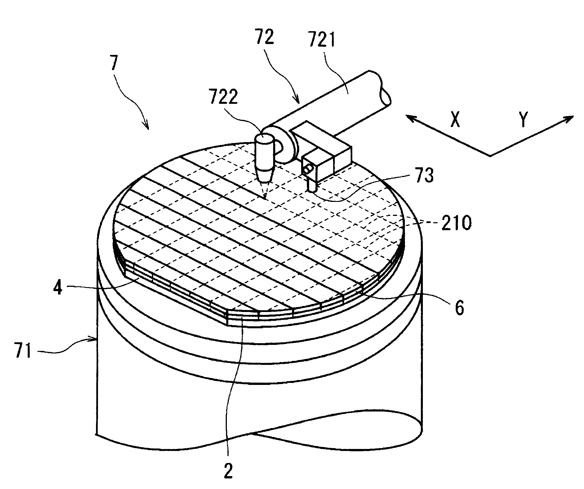
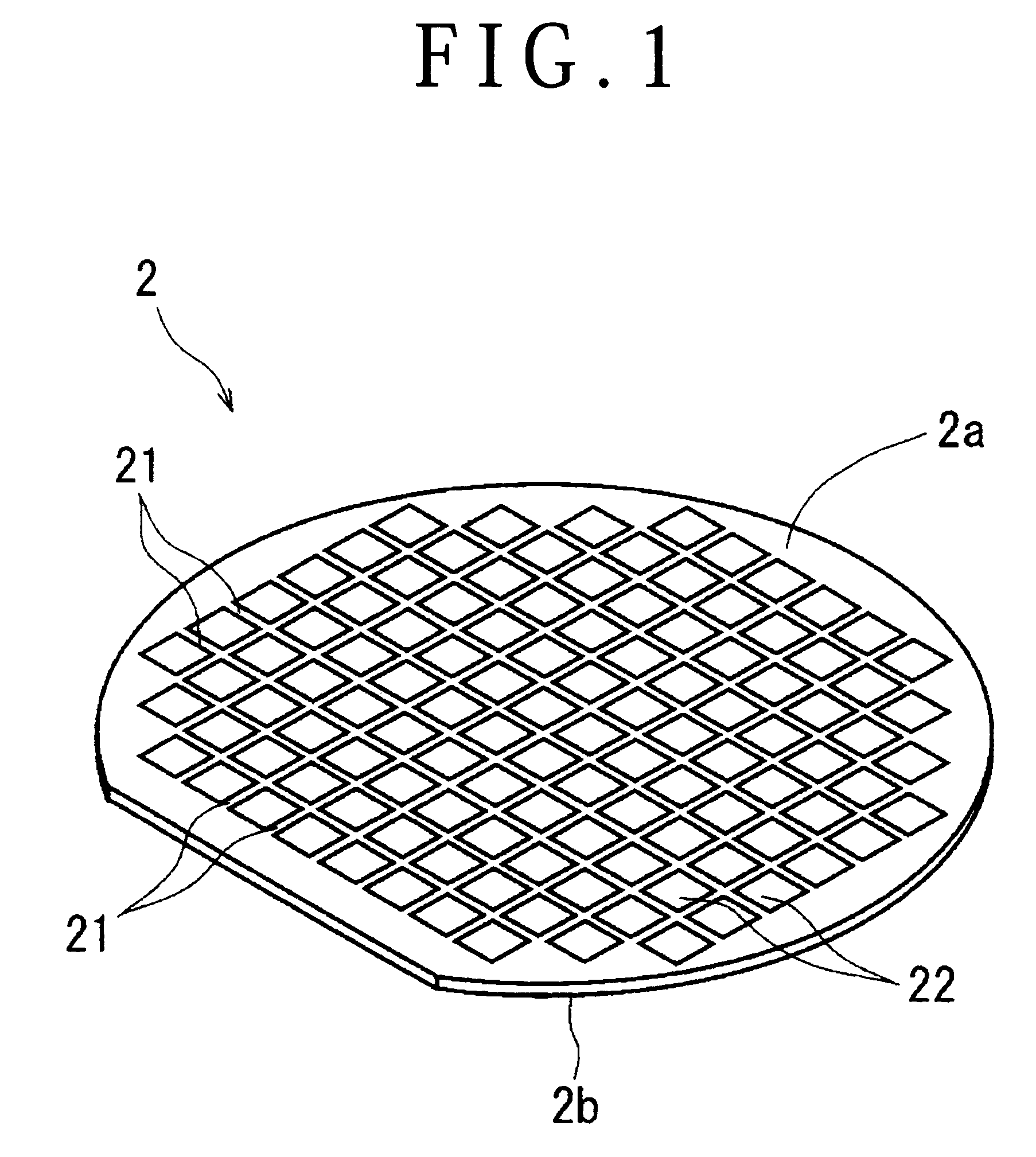
[0027]A preferred embodiment of the device fabrication method according to the present invention will now be described in detail with reference to the attached drawings. FIG. 1 shows a perspective view of a semiconductor wafer 2 as a wafer. For example, the semiconductor wafer 2 shown in FIG. 1 is a silicon wafer having a thickness of 600 μm. A plurality of crossing streets 21 are formed on the front side 2a of the semiconductor wafer 2, thereby partitioning a plurality of rectangular areas in which a plurality of devices 22 such as ICs and LSIs are respectively formed. The procedure of dividing the semiconductor wafer 2 into the individual devices 22 by a dicing before grinding process will now be described.

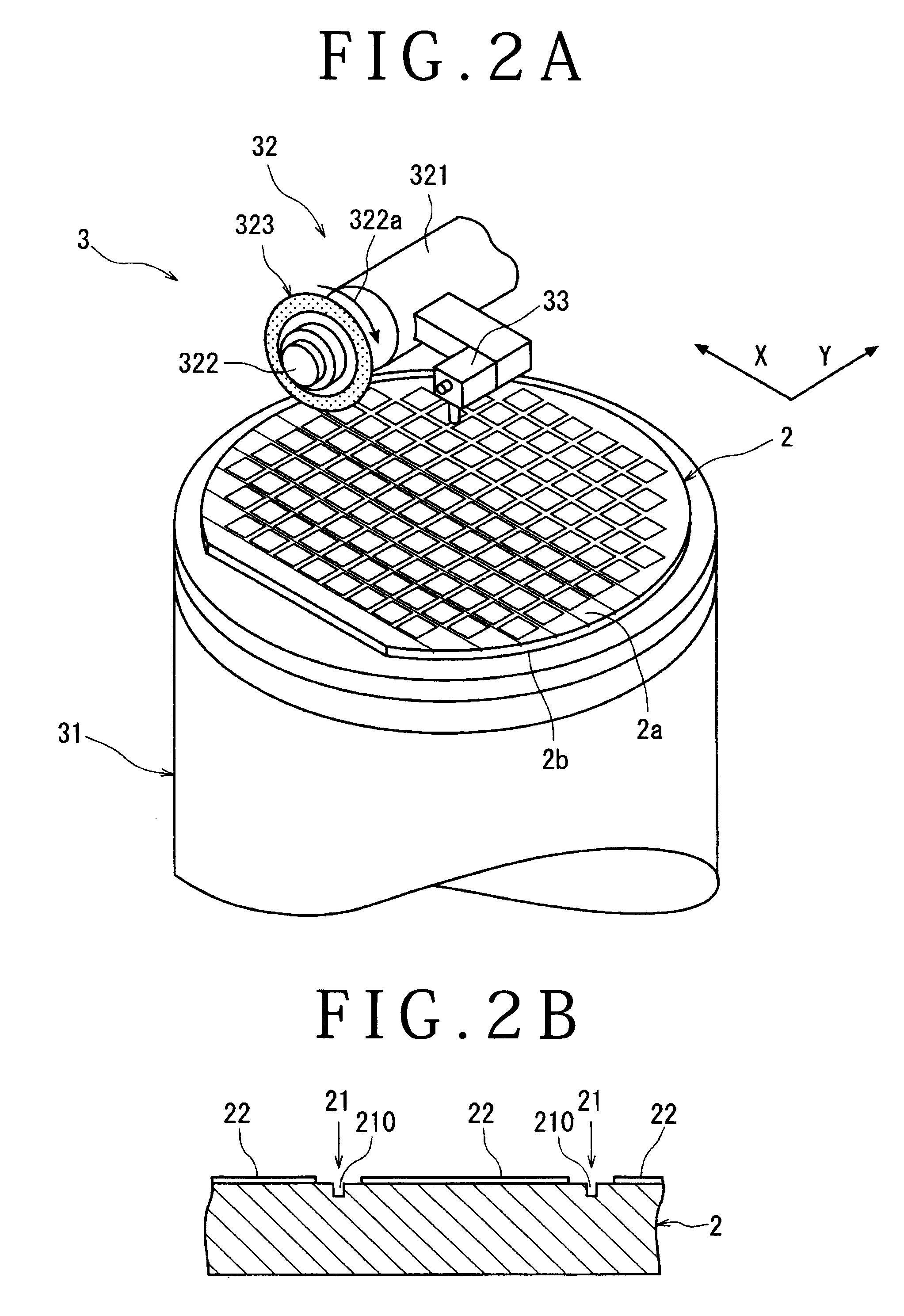
[0028]In the dicing before grinding process for dividing the semiconductor wafer 2 into the individual devices 22, a kerf forming step is first performed in such a manner that the front side 2a of the semiconductor wafer 2 is cut along each street 21 by using a cutting blade to ...


PUM


Abstract

A device fabrication method for fabricating individual devices from a wafer, wherein the back side of each device is covered with an adhesive film for die bonding. The device fabrication method includes a wafer dividing step of dividing the wafer into the individual devices along a plurality of kerfs by using a dicing before grinding process, an adhesive film mounting step of mounting an adhesive film on the back side of the wafer after performing the wafer dividing step, and an adhesive film dividing step of applying a laser beam to the adhesive film along the kerfs after performing the adhesive film mounting step, thereby dividing the adhesive film along the kerfs.

Description

BACKGROUND OF THE INVENTION[0001]1. Field of the Invention[0002]The present invention relates to a device fabrication method for dividing a wafer into individual devices along a plurality of crossing streets formed on the front side of the wafer, wherein the devices are respectively formed in a plurality of regions partitioned by the streets and the back side of each device is covered with an adhesive film for die bonding.[0003]2. Description of the Related Art[0004]In a semiconductor device fabrication process, a plurality of crossing streets (division lines) are formed on the front side of a substantially disk-shaped semiconductor wafer to partition a plurality of regions where devices such as ICs and LSIs are respectively formed, and these regions are separated from each other along the streets to thereby produce the individual devices. As a dividing apparatus for dividing the semiconductor wafer into the individual devices, a cutting apparatus called a dicing apparatus is genera...

Claims


Application Information

Patent Timeline
Patent Type & Authority Patents(United States)
IPC IPC(8): H01L21/46H01L21/78H01L21/301
CPCH01L21/78
Inventor GENDA, SATOSHIKITAHARA, NOBUYASU
Owner DISCO CORP
Why Eureka
Try Eureka