Magnetron control method, magnetron service life judgment method, microwave generation device, magnetron service life judgment device, processing device, computer program, and storage medium

a technology of magnetron and service life, applied in the direction of ohmic-resistance heating, microwave heating, electric/magnetic/electromagnetic heating, etc., can solve the problems of excessive consumption of carbonized layer, reduction of carbonized layer, and expiration of magnetron service life, etc., to prolong the service life of magnetron and high precision

Inactive Publication Date: 2011-03-29
TOKYO ELECTRON LTD
View PDF14 Cites 5 Cited by
  • Summary
  • Abstract
  • Description
  • Claims
  • Application Information

AI Technical Summary

Benefits of technology

The present invention has been devised to solve the above-mentioned problems effectively. It is an object of the present invention to provide a magnetron control method capable of extending a service life of a magnetron by means of controlling a filament temperature of a magnetron with a high precision without complicating the structure thereof; a magnetron service life judgment method; a microwave generation device; a magnetron service life judgment device; a processing apparatus; and a storage medium.
As described above, since the temperature of the filament is controlled to be kept within a specific temperature range by adjusting the current flowing in the filament and / or the voltage applied to the filament, it is possible to extend a service life of a magnetron by means of controlling a filament temperature of a magnetron with a high precision without complicating the structure thereof.

Problems solved by technology

Expiration of the service life of the magnetron is resulted from excessive reduction of this carbonized layer.
For example, if an anode current is increased to enhance the output of the magnetron, the temperature of the filament would be increased as well, resulting in excessive consumption of the carbonized layer.
In the conventional magnetron control method, however, in spite of performing the control of increasing or decreasing the filament voltage in response to the increase or decrease in the output of the magnetron in inverse proportion in order to prevent overheating of the filament, the filament would actually suffer from a considerable variation of its temperature considerably.
In some occasion, the filament would be overheated, and the carbonized layer would be consumed excessively, resulting in a great reduction of the service life of the magnetron.

Method used


Image

  • Magnetron control method, magnetron service life judgment method, microwave generation device, magnetron service life judgment device, processing device, computer program, and storage medium
  • Magnetron control method, magnetron service life judgment method, microwave generation device, magnetron service life judgment device, processing device, computer program, and storage medium
  • Magnetron control method, magnetron service life judgment method, microwave generation device, magnetron service life judgment device, processing device, computer program, and storage medium

Examples


Embodiment Construction

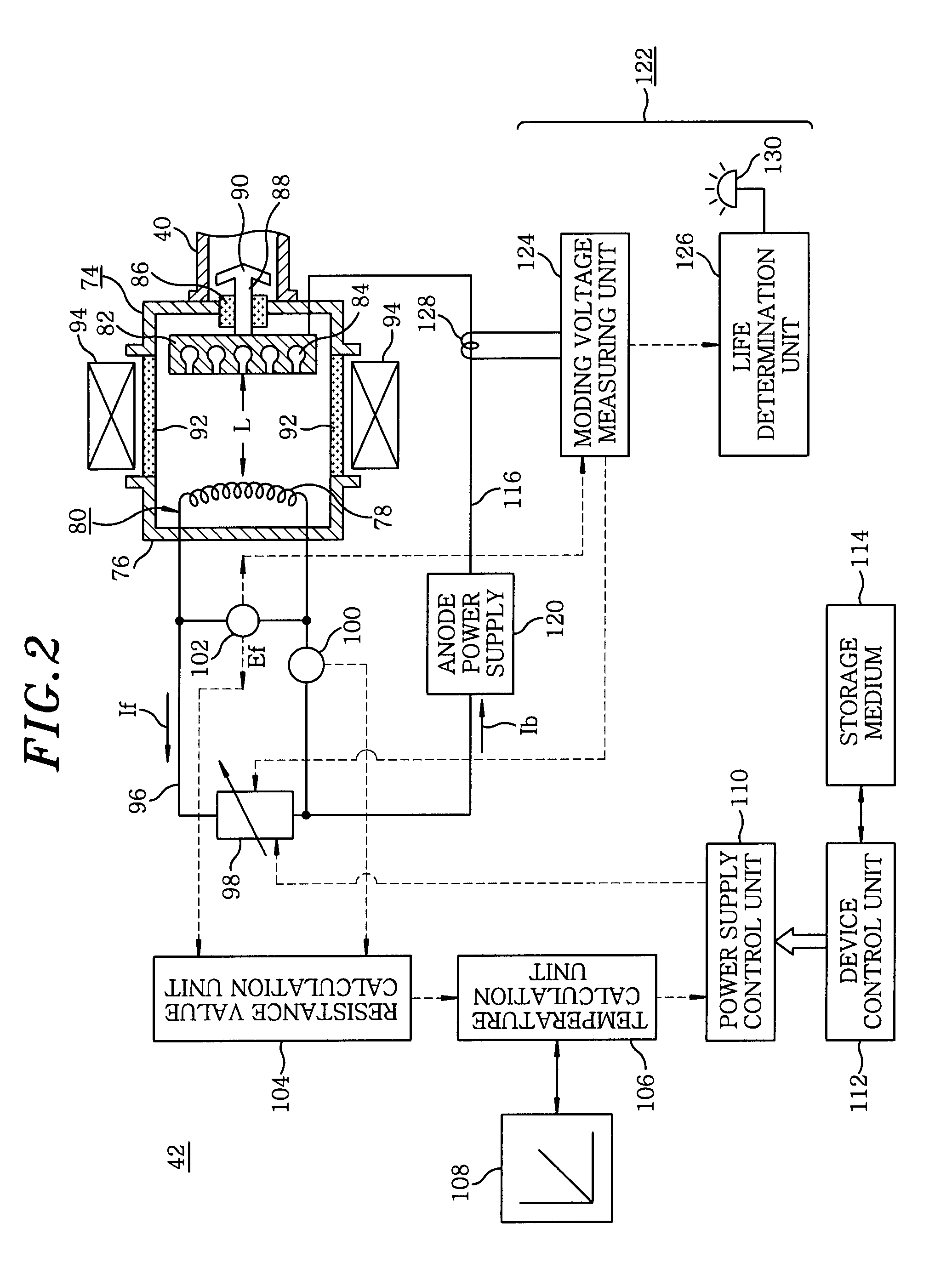
Hereinafter, a magnetron control method, a magnetron service life judgment method, a microwave generation device, a magnetron service life judgment device, a processing device and a storage medium in accordance with a first embodiment of the present invention will be described with reference to the accompanying drawings.

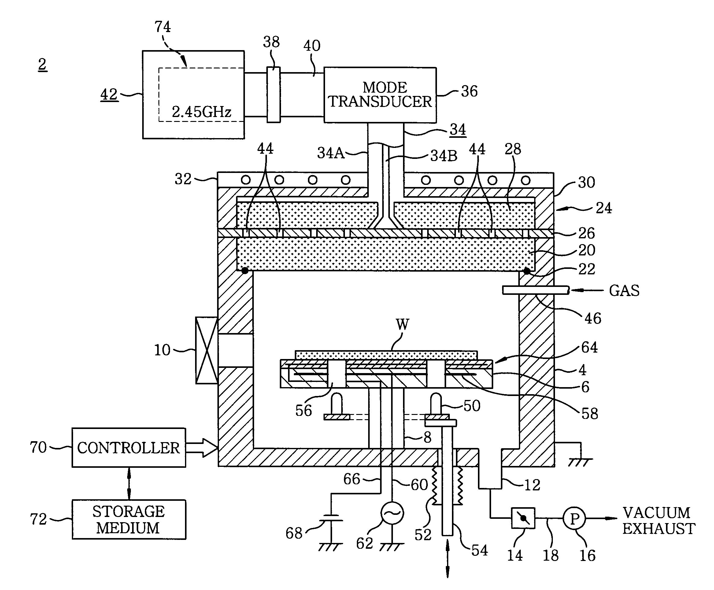
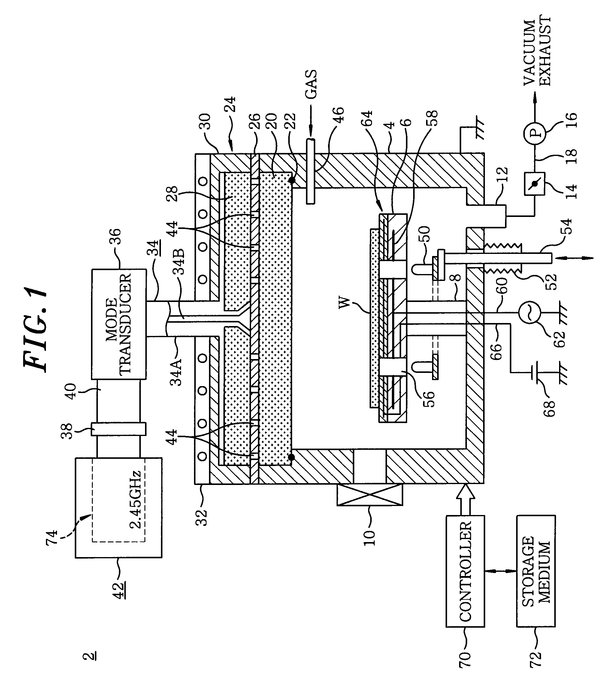
FIG. 1 is a configuration view of an exemplary processing device using a microwave generation device in accordance with the present invention, and FIG. 2 sets forth a block configuration diagram of the microwave generation device. Here, description will be provided for the example of performing an etching process by using a plasma generated by a microwave through the use of the processing device.

As shown, the processing device 2 using plasma includes a cylindrical processing vessel 4 whose sidewall and bottom portion are made of a conductive material such as aluminum or the like. The inside of the processing vessel 4 is configured as a hermetically sealed processing ...


PUM


Abstract

A microwave generation device includes: a magnetron having a cathode containing a filament and an anode containing a hollow resonator arranged to oppose to each other; a filament current measuring unit; and an application voltage measuring unit for measuring voltage applied to the filament. Based on the current and the voltage obtained by the current measuring unit and the voltage measuring unit, a resistance value calculation unit obtains a resistance value of the filament. A temperature calculation unit calculates the filament temperature from the resistance value and the resistance-temperature dependent characteristic. A filament power source is controlled by a power control unit so that the filament temperature is within a predetermined temperature range.

Description

FIELD OF THE INVENTIONThe present invention relates to a processing device for performing a desired processing on a surface of a target object such as a semiconductor wafer by using active species activated by a plasma; a magnetron control method; a magnetron service life judgment method; a microwave generation device; a magnetron service life judgment device; a computer program; and a storage medium.BACKGROUND OF THE INVENTIONIn general, various processes such as a film forming process, a quality modification process, an oxidation / diffusion process, an etching process, and the like are performed on a target object such as a semiconductor wafer to manufacture an integrated circuit of a semiconductor product. Recently, with a demand for further increasing the density of the semiconductor integrated circuit while decreasing the film thickness thereof and a demand for a higher level of miniaturization of the semiconductor integrated circuit and a need to process it at a lower temperatu...

Claims


Application Information

Patent Timeline
Patent Type & Authority Patents(United States)
IPC IPC(8): H01J25/50
CPCH01J37/32192H01J37/32201H05B6/666H05B6/806H05B2206/043H01J23/34H05B6/68H01L21/3065
Inventor KASAI, SHIGERUOSADA, YUKI
Owner TOKYO ELECTRON LTD
Why Eureka
Try Eureka