Optical recording medium
a technology of optical recording medium and blank region, which is applied in the field of optical recording medium, can solve the problems of the difference between the region of the blank region where the record mark is formed and the region of the reflection coefficient where the blank region is sufficiently larg
- Summary
- Abstract
- Description
- Claims
- Application Information
AI Technical Summary
Benefits of technology
Problems solved by technology
Method used
Image
Examples
working examples
Hereinafter, working examples will be set out in order to further clarify the advantages of the present invention.
Working Example 1
An optical recording disk sample #1 was fabricated in the following manner.
A polycarbonate substrate having a thickness of 1.1 mm and a diameter of 120 mm and formed with grooves and lands on the surface thereof was first fabricated by an injection molding process so that the groove pitch was equal to 0.32 μm.
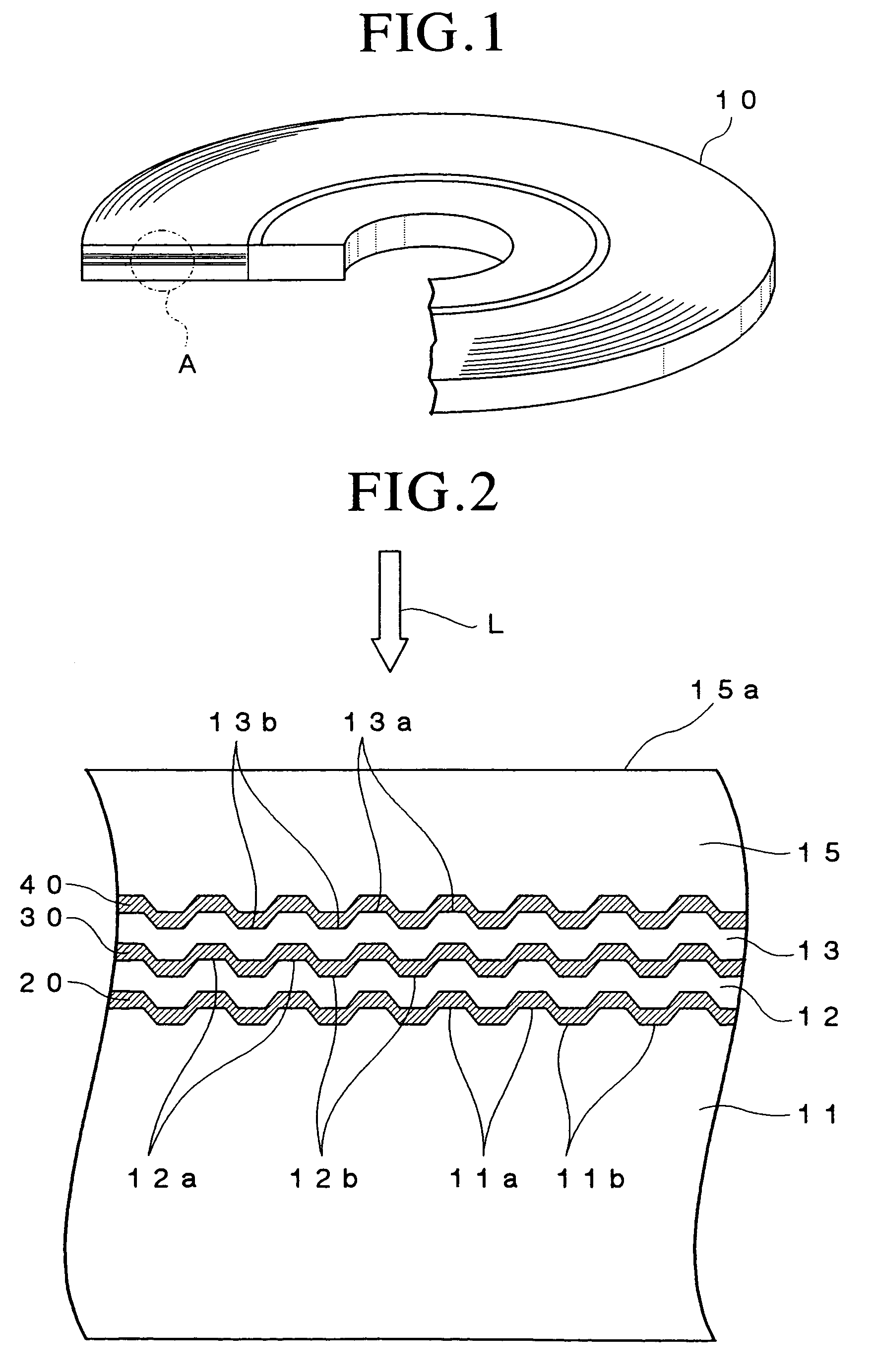
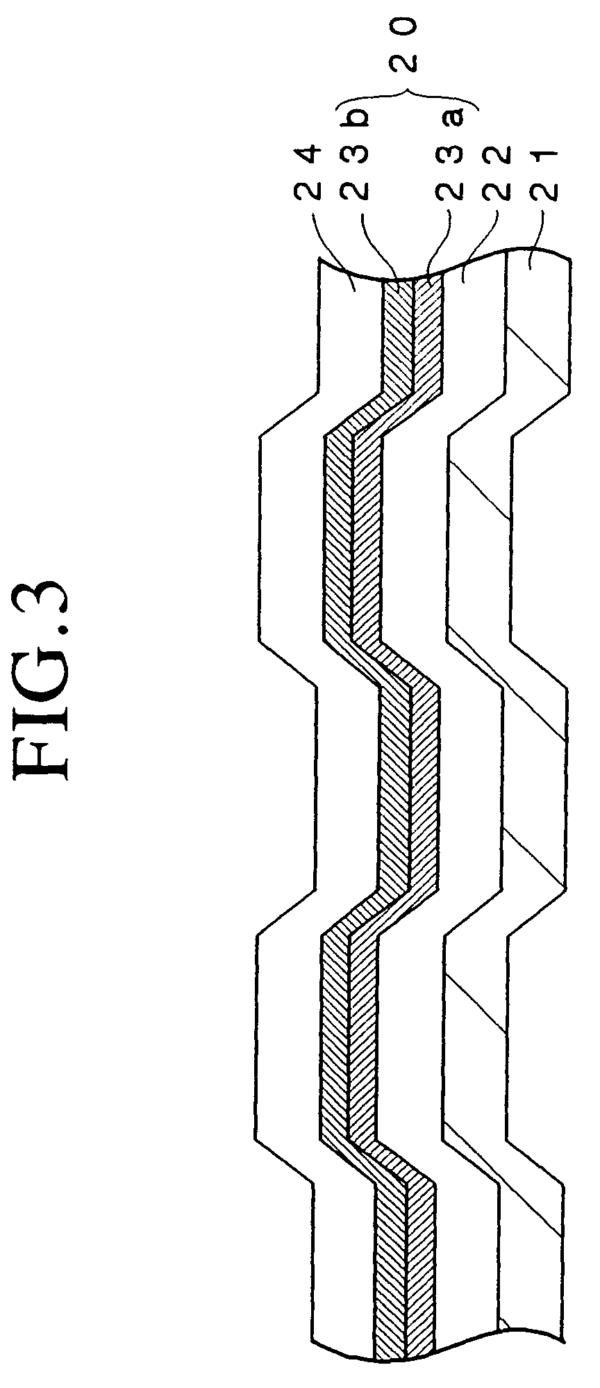
Then, the polycarbonate substrate was set on a sputtering apparatus and a reflective film consisting of an alloy of Ag, Pd and Cu and having a thickness of 100 nm, a second dielectric film containing a mixture of ZnS and SiO2 and having a thickness of 39 nm, a first recording film containing Cu as a primary component, added with 23 atomic % of Al and 13 atomic % of Au and having a thickness of 5 nm, a second recording film containing Si as a primary component and having a thickness of 5 nm and a first dielectric film containing the mixture of ZnS an...
working example 2
A polycarbonate substrate having a thickness of 1.1 mm and a diameter of 120 mm was set on a sputtering apparatus and a recording layer having a thickness of 18 nm was formed on the polycarbonate substrate by the sputtering process using a mixture target consisting of the mixture of ZnS and SiO2 and a target consisting of Mg, thereby fabricating an optical recording disk sample #2.
The mole ratio of ZnS to SiO2 in the mixture of ZnS and SiO2 contained in the target was 80:20.
The composition of the recording layer of the optical recording disk sample #2 was measured similarly to in Working Example 1. It was found that the recording layer contained 21.5 atomic % of Zn, 10.1 atomic % of Si, 20.8 atomic % of Mg, 20.1 atomic % of O and 27.5 atomic % of S.
Then, a polycarbonate substrate having a thickness of 1.1 mm and a diameter of 120 mm was set on a sputtering apparatus and a recording layer having a thickness of 24 nm was formed on the polycarbonate substrate by the sputtering process ...
working example 3
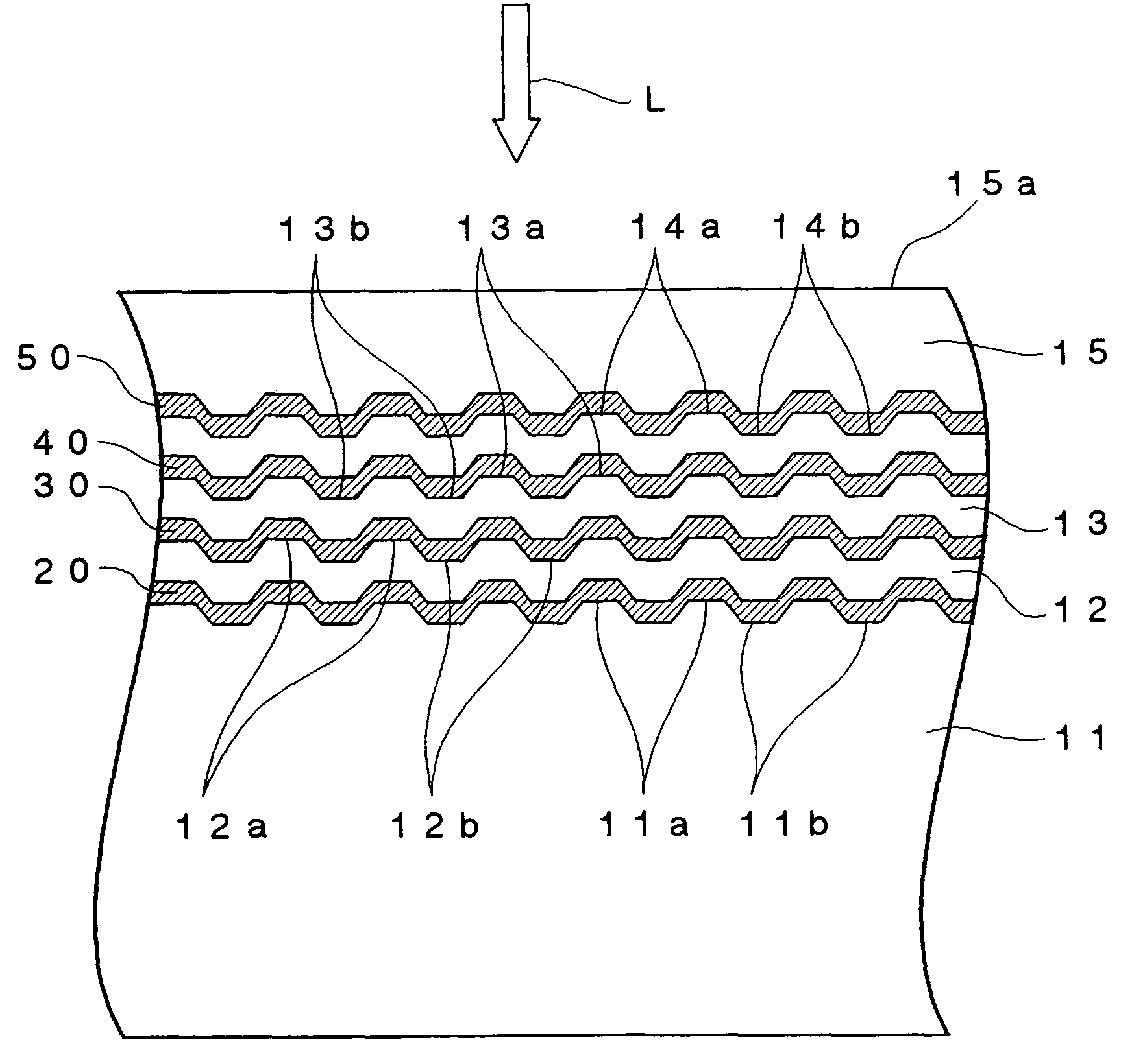
An optical recording disk sample #5 was fabricated in the manner of the optical recording disk sample #1 except that when the second recording layer, the third recording layer and the fourth recording layer were formed using a target consisting of a mixture of La2O3, SiO2 and Si3N4 whose mole ratio was 20:30:50 instead of the target consisting of the mixture of ZnS and SiO2 was 80:20 so that the second recording layer had thickness of 28 nm, the third recording layer had a thickness of 18 nm and the fourth recording layer had a thickness of 15 nm.
The compositions of the second recording layer, the third recording layer and the fourth recording layer of the optical recording disk sample #5 were measured similarly to in Working Example 1. It was found that each of the second recording layer, the third recording layer and the fourth recording layer contained 6.2 atomic % of La, 24.1 atomic % of Si, 23.1 atomic % of Mg, 24.6 atomic % of O and 22.0 atomic % of N.
Since O is contained in t...
PUM
 Abstract
Description
Claims
Application Information


