High speed low power annular magnetic devices based on current induced spin-momentum transfer

a technology of annular magnetic devices and current induced spin, applied in the field of magnetic devices, can solve the problems of limiting the density of memory, slow device operation, memory operation errors, etc., and achieve the effects of reducing power consumption, improving reliability, and speed of operation

Inactive Publication Date: 2008-05-15
NEW YORK UNIV
View PDF58 Cites 159 Cited by
  • Summary
  • Abstract
  • Description
  • Claims
  • Application Information

AI Technical Summary

Benefits of technology

[0010]In view of the limitations associated with conventional designs of devices that use spin-momentum transfer, an object of the present invention is to provide a structure that is optimal for a magnetic memory or magnetic information processing device.
[0011]It is another object of the present invention to produce a magnetic device that has advantages in terms of speed of operation.
[0012]It is a further object of the present invention to produce a magnetic device that has advantages in terms of reliability.
[0013]It is a further object of the present invention to produce a magnetic device that requires lower power to operate.
[0014]It is a further object of the present invention to produce a magnetic device that has advantages in terms of the stability of the stored information.
[0019]This demagnetizing field forces the magnetization vector of the free magnetic layer to precess, i.e., for the magnetization direction to rotate around the direction of the demagnetization magnetic field. The demagnetizing field also determines the rate of precession. A large demagnetizing field results in a high precession rate, which is an optimal condition for fast magnetic switching. An advantage of this magnetic device is that random fluctuating forces or fields are not necessary to initiate or control the magnetic response of the layers.

Problems solved by technology

This cross-talk will limit the density of the memory and / or cause errors in memory operations.
Further, the magnetic fields generated by such wires are limited to about 0.1 Tesla at the position of the electrodes, which leads to slow device operation.
Importantly, conventional memory designs also use stochastic (random) processes or fluctuating fields to initiate the switching events, which is inherently slow and unreliable (see, for example, R. H. Koch et al., Phys. Rev. Lett. 84, 5419 (2000)).
However, the proposed mechanism was purely theoretical.
However, the proposed devices are slow and rely on fluctuating magnetic fields and stochastic processes to initiate magnetization switching.
Further, large current densities are needed to switch the devices.
However, the devices proposed were unreliable, as there was little consistency with regard to device characteristics.

Method used


Image

  • High speed low power annular magnetic devices based on current induced spin-momentum transfer
  • High speed low power annular magnetic devices based on current induced spin-momentum transfer
  • High speed low power annular magnetic devices based on current induced spin-momentum transfer

Examples


example

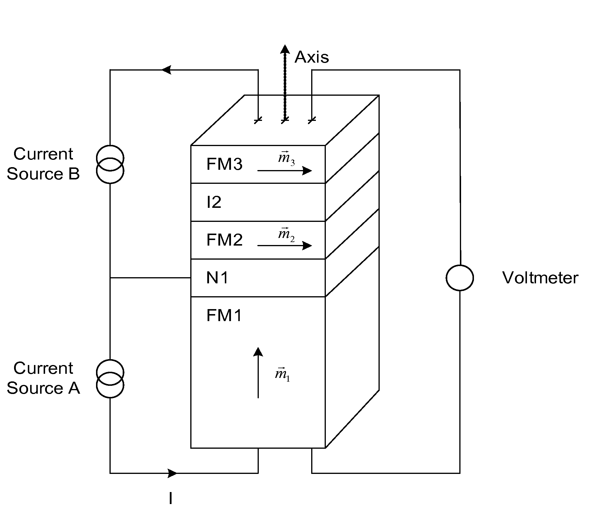
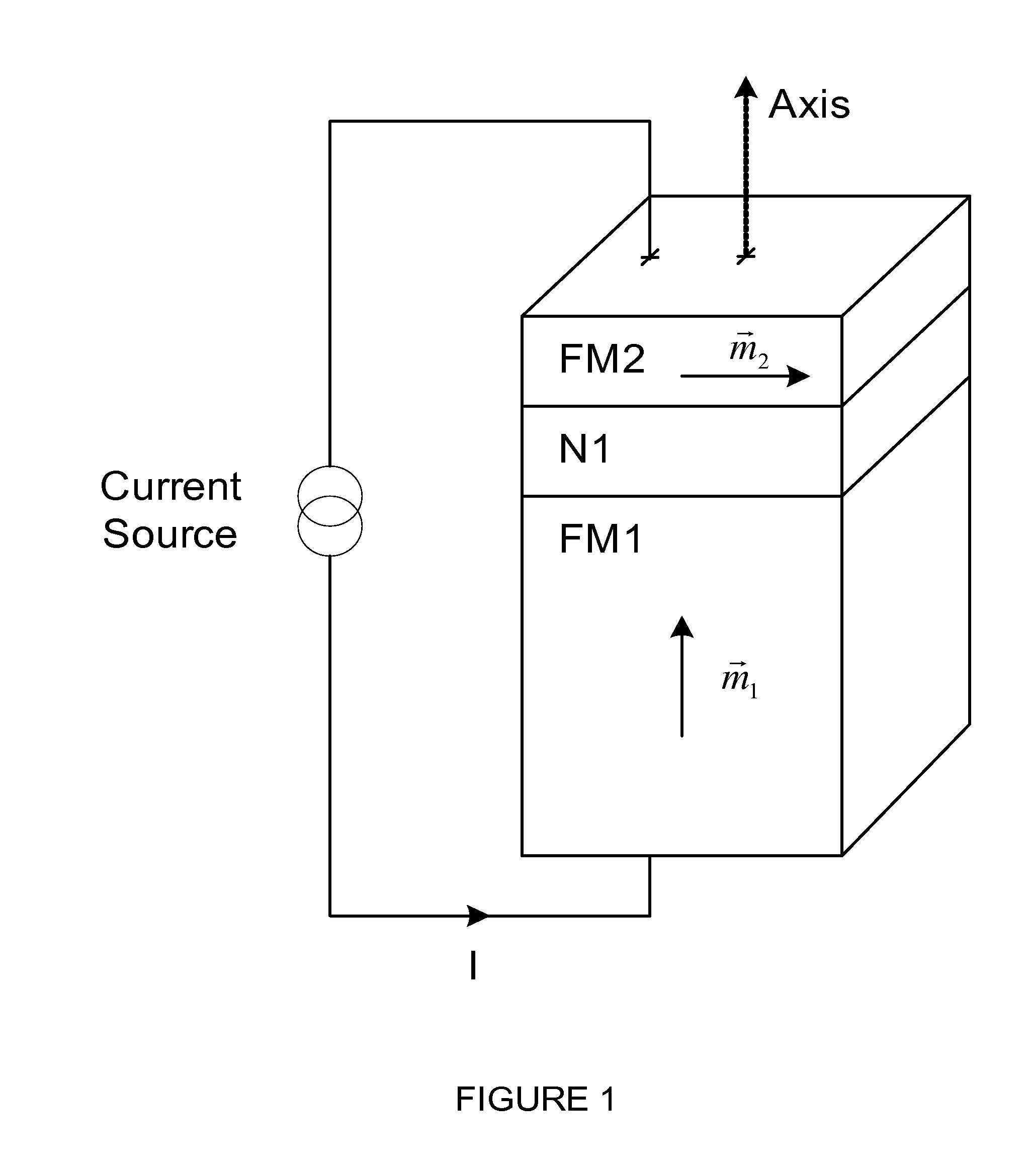
[0071]The operation of the magnetic device was simulated using Landau-Lifzshitz Gilbert equations including a spin-transfer torque.

[0072]FIG. 8 shows the amplitude of the current input applied to the magnetic memory device starting at an initial time t=0 and ending at t=30 picoseconds. This current input comprises two current pulses similar to the current input shown in FIGS. 3A and 6A.

[0073]A 16-picosecond positive current pulse is applied to the magnetic memory device to start the precession of the magnetization vector {right arrow over (m)}2 of the free magnetic layer FM2. After this 16-picosecond current pulse, a 14-picosecond negative current pulse is applied to the magnetic memory device to stop the precession of the magnetization vector {right arrow over (m)}2 of the free magnetic layer FM2 to achieve a desired state of the magnetization vector {right arrow over (m)}2. For magnetic memory devices, the precession is stopped after achieving a 180° rotation of the magnetization ...


PUM

PropertyMeasurementUnit
thicknessesaaaaaaaaaa
magnetic fieldsaaaaaaaaaa
currentaaaaaaaaaa

Abstract

A high speed and low power method to control and switch the magnetization direction and / or helicity of a magnetic region in a magnetic device for memory cells using spin polarized electrical current. The magnetic device comprises a reference magnetic layer with a fixed magnetic helicity and / or magnetization direction and a free magnetic layer with a changeable magnetic helicity. The fixed magnetic layer and the free magnetic layer are preferably separated by a non-magnetic layer, and the reference layer includes an easy axis perpendicular to the reference layer. A current can be applied to the device to induce a torque that alters the magnetic state of the device so that it can act as a magnetic memory for writing information. The resistance, which depends on the magnetic state of the device, is measured to thereby read out the information stored in the device.

Description

[0001]This patent application is a continuation-in-part of U.S. patent application Ser. No. 11 / 498,303, filed Aug. 1, 2006, which is a continuation in part of U.S. patent application Ser. No. 11 / 250,791, filed Oct. 13, 2005, allowed Nov. 14, 2006, and issued as U.S. Pat. No. 7,170,778 on Jan. 30, 2007 which is a continuation of U.S. patent application Ser. No. 10 / 643,762 filed Aug. 19, 2003, allowed Sep. 12, 2005, and issued as U.S. Pat. No. 6,980,469 on Dec. 27, 2005.[0002]This invention was made with government support under Contract Number NSF-DMR-0405620 entitled “Nanoscale Spin Transfer Devices and Materials” and Contract Numbers NSF-PHY-0351964 and NSF-PHY-0601179 entitled “Noise-Induced Escape in Multistable Systems” awarded by the National Science Foundation, and Contract Number ONR N0014-02-1-0995 entitled “Gate Controlled Ferromagnetism in Semiconductor Nanostructures” awarded by the Office of Naval Research of the Department of Defense. The government has certain rights i...

Claims


Application Information

Patent Timeline
Patent Type & Authority Applications(United States)
IPC IPC(8): G11B5/33
CPCG11C11/5607G11C11/16G11C11/161G11C11/1673G11C11/1675H10N50/01H10N50/10
Inventor KENT, ANDREWOZYILMAZ, BARBAROSGARCIA, ENRIQUE GONZALEZ
Owner NEW YORK UNIV
Why Eureka
Try Eureka