Method and device for high sensitivity detection of the presence of DNA and other probes

a technology applied in the field of high sensitivity detection of the presence of dna and other probes, can solve the problems of limited external optical detection of a specific opaque label such as silver, long processing time, and possibility of false positive readings

a technology applied in the field of high sensitivity detection of the presence of dna and other probes, can solve the problems of limited external optical detection of a specific opaque label such as silver, long processing time, and possibility of false positive readings

US7943394B2Inactive Publication Date: 2011-05-17UNIVERSITE CATHOLIQUE DE LOUVAIN

Image

  • Method and device for high sensitivity detection of the presence of DNA and other probes
  • Method and device for high sensitivity detection of the presence of DNA and other probes
  • Method and device for high sensitivity detection of the presence of DNA and other probes

Examples


example

Materials and Processes

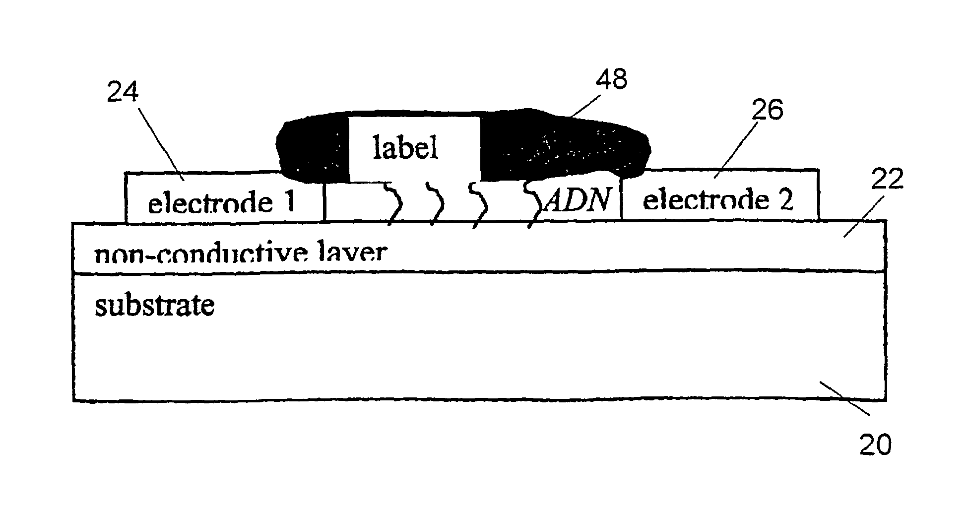
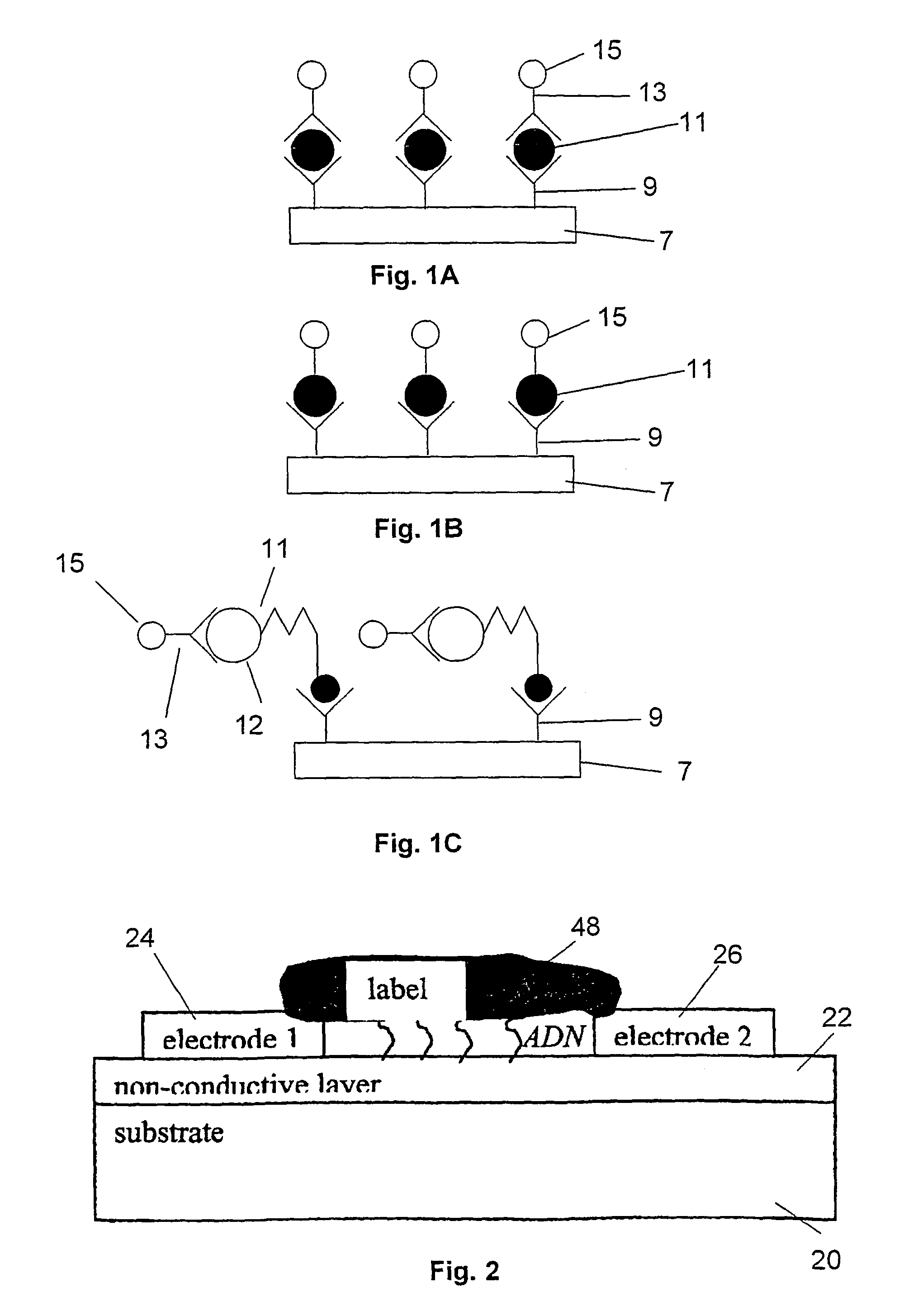
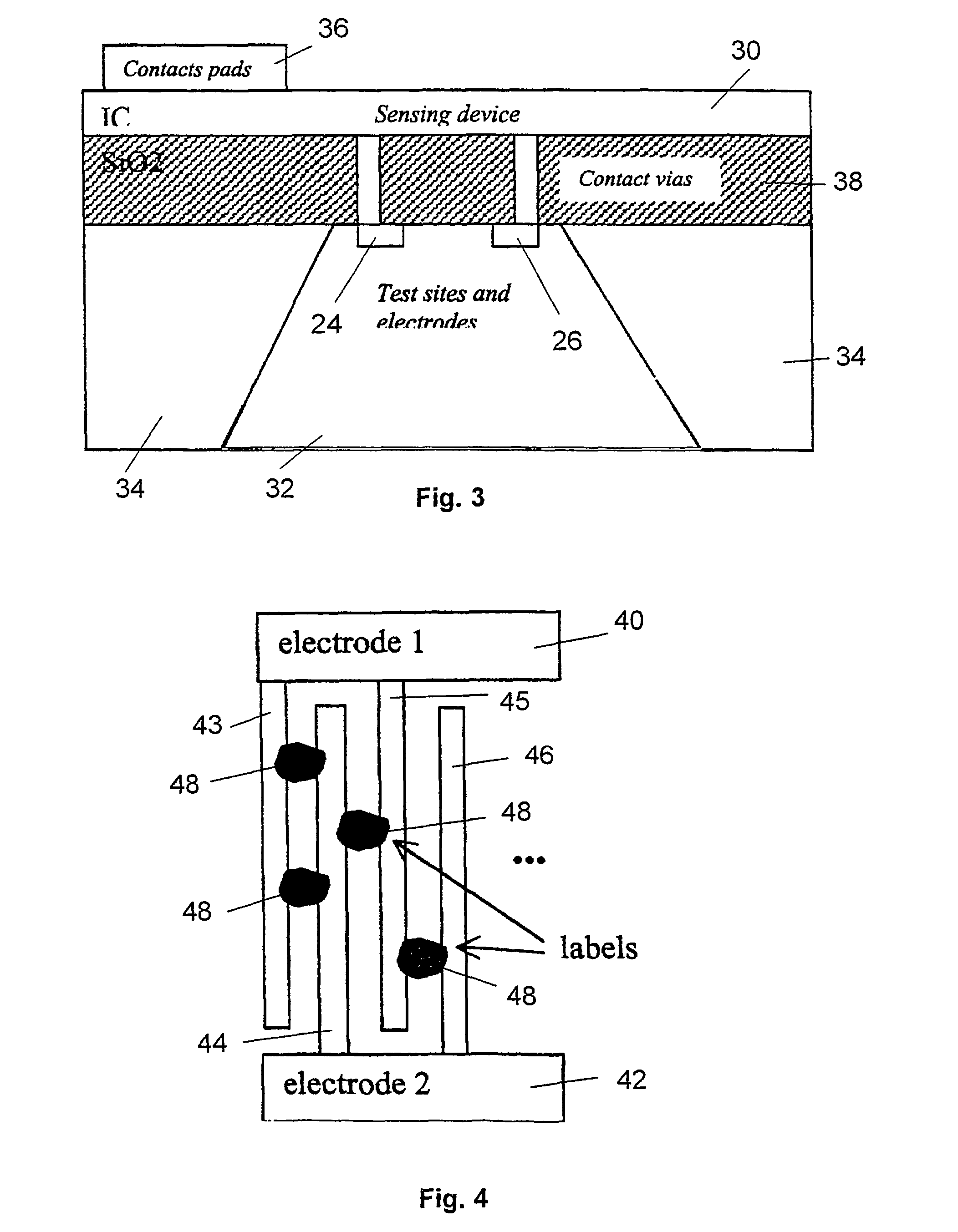
[0110]Standard P-doped Si wafers were used to make the chips according to the present invention. In order to insulate the electrodes from the substrate and lowering the parasitic bulk effects, a 400 nm thick thermal wet oxide (SiO2) was grown—in fact previous experiments showed that this kind of material enhanced the binding of DNA to the support. The growing temperature and time of the SiO2 were 1000° C. and 1 h 16 min respectively. To guaranty a pure wet oxide, a short delay of around 1 minute only was left between oxygen and hydrogen valves opening.

[0111]The electrodes were manufactured with pure aluminium, by means of a lift-off process. This was preferred to an etching method because previous tests used to show a non-specific silver precipitation on a 240 nm-thick silicon oxide in the second case, after deposition and plasma etch of 1 μm of {Al+2% Si}. In the lift-off process, an aluminium thickness of 500 nm was used, and nitric acid was used for the pho...


PUM

PropertyMeasurementUnit
sizeaaaaaaaaaa
distanceaaaaaaaaaa
distanceaaaaaaaaaa

Abstract

The present invention provides a method for capacitive detection of the presence of target sample on a substrate, which comprises the steps of: binding a target sample to selective binding sites on the substrate, the target sample being directly or indirectly labeled with conductive labels, and sensing the presence of the bound conductive labels to a binding site to thereby determine the presence of the target sample. The sensing step is carried out by a capacitive detection of the presence of the conductive labels. The present invention also provides a capacitive sensor device for determining the presence of a target sample. Conductive labels are directly or indirectly couplable to the target sample. The capacitive sensor device comprises a substrate having attached thereto a binding site able to selectively bind a target sample, a capacitive sensor element, and sensing circuitry for determining the presence of a target sample bound to the binding site by application of electrical signals to a capacitive sensor element. The capacitive sensor element comprises a set of at least two electrodes with non-conductive surfaces in a region associated with the binding site.

Description

CROSS REFERENCE TO RELATED APPLICATIONS[0001]This application is the U.S. National Stage of International Application No. PCT / BE2003 / 000109, filed Jun. 24, 2003, which was published in English under PCT Article 21(2), and which claims the benefit of European patent application 02447122.9, filed Jun. 24, 2002.TECHNICAL FIELD OF THE INVENTION[0002]The present invention relates to a method and apparatus for sensing of the presence of a molecular species or substance bound to a binding site, especially by means of conductive labels. In particular it relates to apparatus and methods for capacitive detection of binding of biological molecules on a micro-array or biochip.BACKGROUND OF THE INVENTION[0003]The introduction of micro-arrays or biochips is revolutionising the analysis of DNA (desoxyribonucleic acid), RNA (ribonucleic acid), proteins, other molecules, e.g. herbicides and pesticides, or other micro- or nanomaterials, e.g. microcarriers such as beads. Applications are, for example,...

Claims


Application Information

Patent Timeline
17 May 2011
Publication
US7943394B2
IPC
G01N33/566; C12Q1/68; G01N27/02; G01N27/22; G01N33/543
CPC
G01N27/221; G01N27/226; G01N33/5438; Y10T436/163333; Y10T436/173845; Y10T436/147777
Inventors
FLANDRE, DENIS; HAGELSIEB, LUIS MORENO