

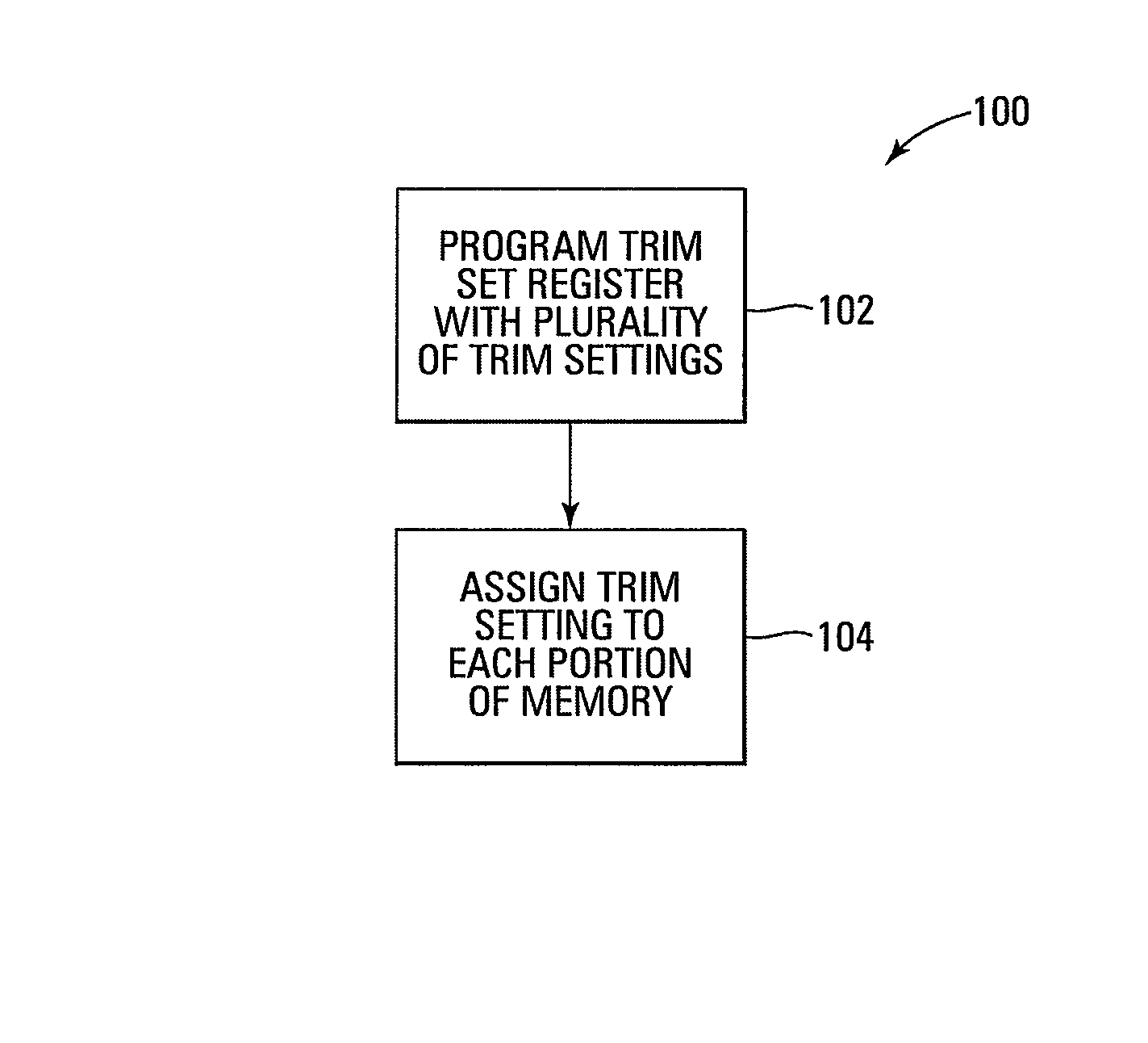
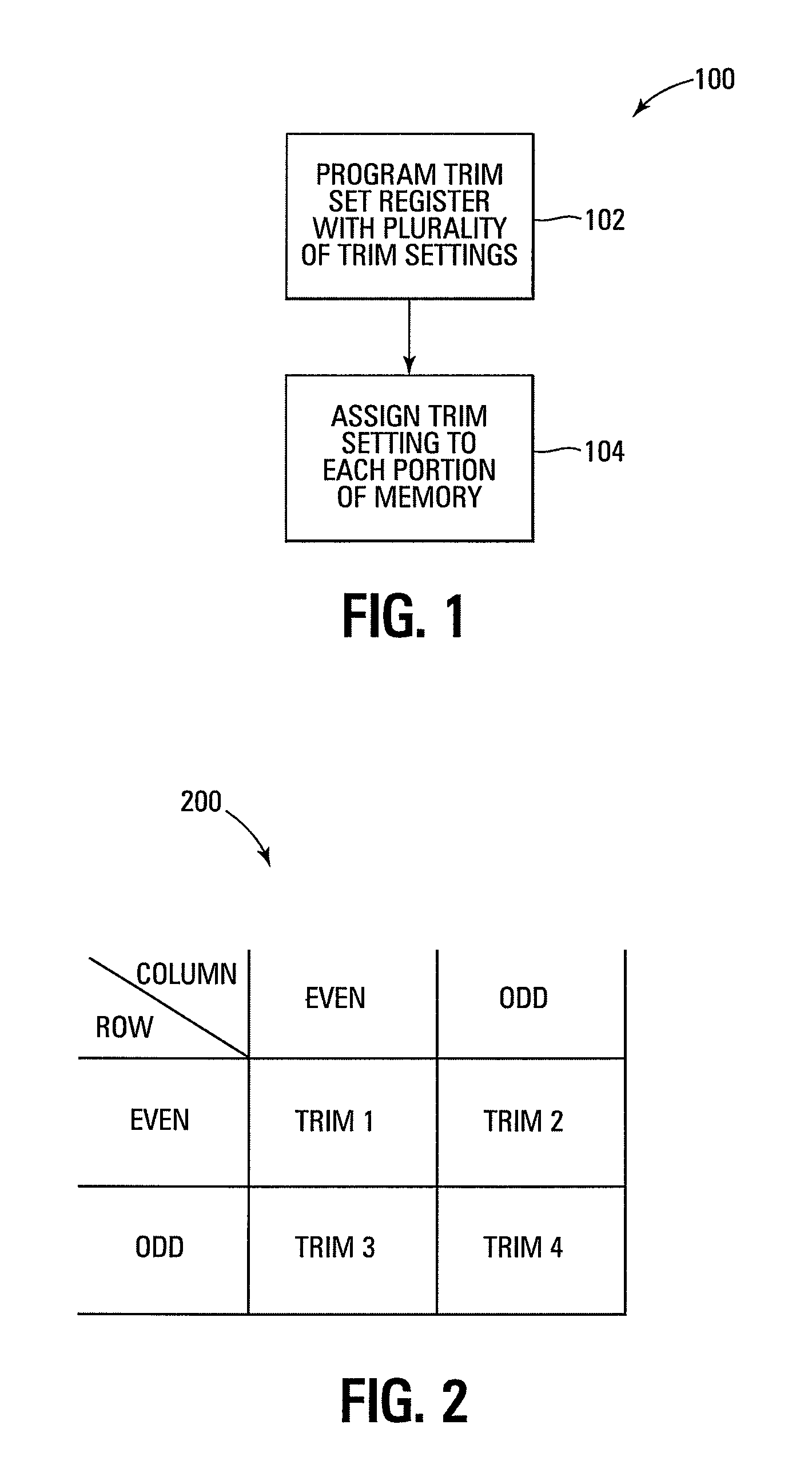
Program and read trim setting
a trim setting and program technology, applied in the field of flash memory devices, can solve the problems of increasing the critical dimension difference between even and odd columns and rows, reducing the uniformity of side wall oxides and etching, and single trim setting is not suitable for all pages, so as to achieve the effect of increasing the program reliability
- Summary
- Abstract
- Description
- Claims
- Application Information
AI Technical Summary
Benefits of technology
Problems solved by technology
Method used
Image

Examples
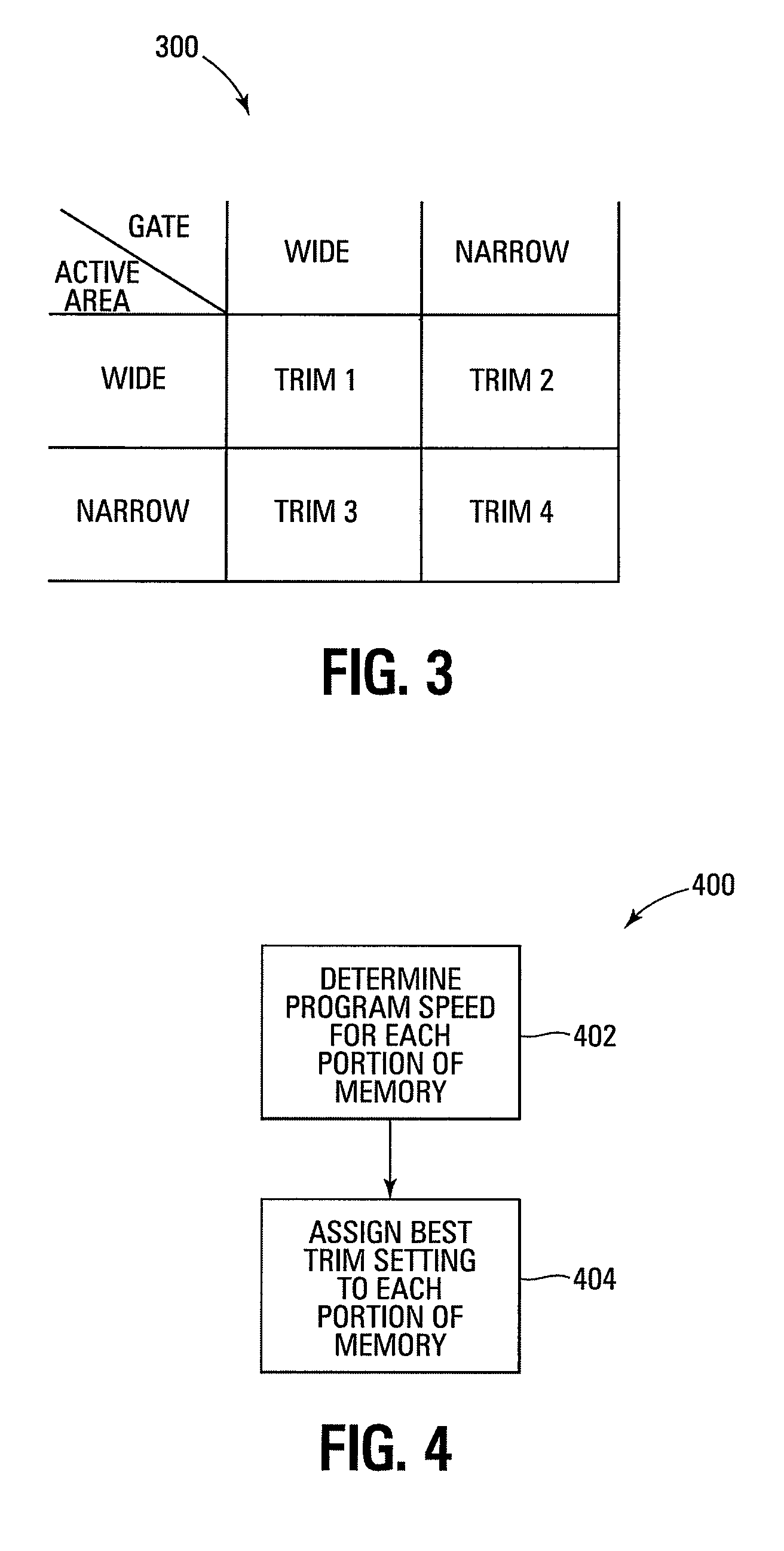
embodiment 300
[0026]In another embodiment 300, the trim settings are assigned to wide and narrow active area and gate configuration combinations as shown in FIG. 3. Another embodiment of the present invention provides trim settings identified with wide active areas for the lines and wide gates for transistors in the portion (trim 1), wide active areas for the lines and narrow gates for transistors in the portion (trim 2), narrow active areas for the lines and wide gates for transistors in the portion (trim 3), and narrow active areas for the lines and narrow gates for transistors in the portion (trim 4). Each trim set is independent and is used for the specific wide / narrow combination. Each trim set has three parameters, a program voltage trim parameter, a step up voltage trim parameter, and a program pulse width trim parameter. The four separate trim settings allow for separate settings for faster or slower programming times based on for instance geometry of the lines. Each page in this embodime...
embodiment 450
[0033]FIG. 4A is an embodiment 450 of another array image of possible trim settings in a memory. Array 450 is shown with 2048 blocks. In this embodiment, blocks 452 (labeled as blocks 0, 1, 2, 2045, 2046, and 2047) are edge blocks. Blocks 454 (labeled as blocks 3, 4, 5, . . . , 2042, 2043, and 2044) are center blocks. In this embodiment, edge blocks 452 and center blocks 454 have different trim settings. In this embodiment, the number of different trim settings is two. The trim settings are therefore in this embodiment dependent upon block array location.
[0034]FIG. 5 is a functional block diagram of a memory device 500, such as a flash memory device, of one embodiment of the present invention, which is coupled to a processor 510. The memory device 500 and the processor 510 may form part of an electronic system 520. The memory device 500 has been simplified to focus on features of the memory that are helpful in understanding the present invention. The memory device includes an array ...
PUM
 Abstract
Description
Claims
Application Information