Layered chip package with wiring on the side surfaces

a layer chip and side surface technology, applied in the direction of electrical equipment, semiconductor devices, semiconductor/solid-state device details, etc., can solve the problems of increasing the cost of the layer chip package, affecting the high-speed operation of the circuit, and difficulty in reducing the distance between the electrodes, so as to reduce the problem of malfunctioning chips, reduce the cost, and disable the use of malfunctioning chips.

Inactive Publication Date: 2011-06-28
HEADWAY TECH INC +2
View PDF10 Cites 17 Cited by
  • Summary
  • Abstract
  • Description
  • Claims
  • Application Information

AI Technical Summary

Benefits of technology

[0021]It is an object of the present invention to provide a layered chip package and its manufacturing method that make it possible to implement, at low cost, a layered chip package including a plurality of chips stacked, the layered chip package being capable of disabling the use of a malfunctioning chip while reducing problems attributable to wiring connected to the malfunctioning chip, and also capable of performing equally well irrespective of whether a malfunctioning chip is included or not.
[0050]According to the method of manufacturing a layered chip package of the present invention, or the first or second layered chip package of the present invention, it is possible to disable the use of a malfunctioning chip while reducing problems attributable to wiring connected to the malfunctioning chip.
[0051]According to the method of manufacturing a layered chip package of the present invention, the layered substructure is used to fabricate the pre-main-body stack which is a stack of a predetermined two or greater number of pairs of layer portions including at least one specific pair of layer portions, and the main body is fabricated by stacking at least one additional first-type layer portion together with the pre-main-body stack, the number of the at least one additional first-type layer portion being equal to the number of the at least one specific pair of layer portions included in the pre-main-body stack. The present invention thus makes it possible to implement, at low cost, a layered chip package that performs equally well irrespective of whether a malfunctioning chip is included or not.
[0052]In the first layered chip package according to the present invention, the number of the specific pairs of layer portions is an even number. When a stack of a predetermined number of pairs of layer portions includes at least one specific pair of layer portions, the main body of this layered chip package is formed by stacking at least one additional specific pair of layer portions together with the foregoing stack, the number of the at least one additional specific pair of layer portions being equal to the number of the at least one specific pair of layer portions included in the stack. The present invention thus makes it possible to implement, at low cost, a layered chip package that performs equally well irrespective of whether a malfunctioning chip (the chip in the second-type layer portion) is included or not.
[0053]In the second layered chip package according to the present invention, the main body includes at least nine layer portions stacked, the at least nine layer portions consisting of eight first-type layer portions and at least one second-type layer portion. The at least nine layer portions include at least four pairs of layer portions, and the at least four pairs of layer portions include at least one specific pair of layer portions. When a stack of four pairs of layer portions includes at least one specific pair of layer portions, the main body is formed by stacking at least one additional first-type layer portion together with the foregoing stack, the number of the at least one additional first-type layer portion being equal to the number of the at least one specific pair of layer portions included in the stack. The present invention thus makes it possible to implement, at low cost, a layered chip package that performs equally well irrespective of whether a malfunctioning chip (the chip in the second-type layer portion) is included or not.

Problems solved by technology

The wire bonding method has a problem that it is difficult to reduce the distance between the electrodes so as to avoid contact between wires, and a problem that high resistances of the wires hamper a high-speed operation of a circuit.
Unfortunately, however, the through electrode method requires a large number of steps for forming the through electrodes in chips, and consequently increases the cost for the layered chip package.
Consequently, voids or keyholes are prone to occur in the through electrodes due to poor filling of the holes with metal, so that the reliability of wiring formed by the through electrodes tends to be reduced.
When the upper and lower chips are joined to each other at high temperatures, however, misalignment between the upper and lower chips can occur due to expansion and contraction of the chips, which often results in electrical connection failure between the upper and lower chips.
The manufacturing method disclosed in U.S. Pat. No. 5,953,588 involves a number of process steps and this raises the cost for the layered chip package.
This is also a factor that raises the cost for the layered chip package.
According to this multilayer module, however, it is impossible to increase the proportion of the area occupied by the electronic element in each active layer, and consequently it is difficult to achieve higher integration.
However, if, for example, a chip that includes a control circuit and a plurality of memory cells has become defective due to a wiring failure in the control circuit and cannot function normally even by employing the redundancy technique, this defective chip is unusable.
In this case, replacing the defective chip with a non-defective one raises the cost for the layered chip package.
However, disabling a defective chip in a layered chip package involves a problem as described below.
The wiring connecting the defective chip to the plurality of terminals of the layered chip package generates a capacitance or inductance that is unwanted for a device implemented by the layered chip package, such as a memory device, and / or generates a stray capacitance between itself and other wiring connected to non-defective chips.
This is a hindrance to increasing the operation speed of the device such as the memory device.
In addition, if a layered chip package including a predetermined number of chips is able to implement a memory device having a desired memory capacity when all the chips included in the layered chip package are non-defective, it is impossible to implement the memory device having the desired memory capacity by simply disabling a defective chip included in the layered chip package.

Method used


Image

  • Layered chip package with wiring on the side surfaces
  • Layered chip package with wiring on the side surfaces
  • Layered chip package with wiring on the side surfaces

Examples


first embodiment

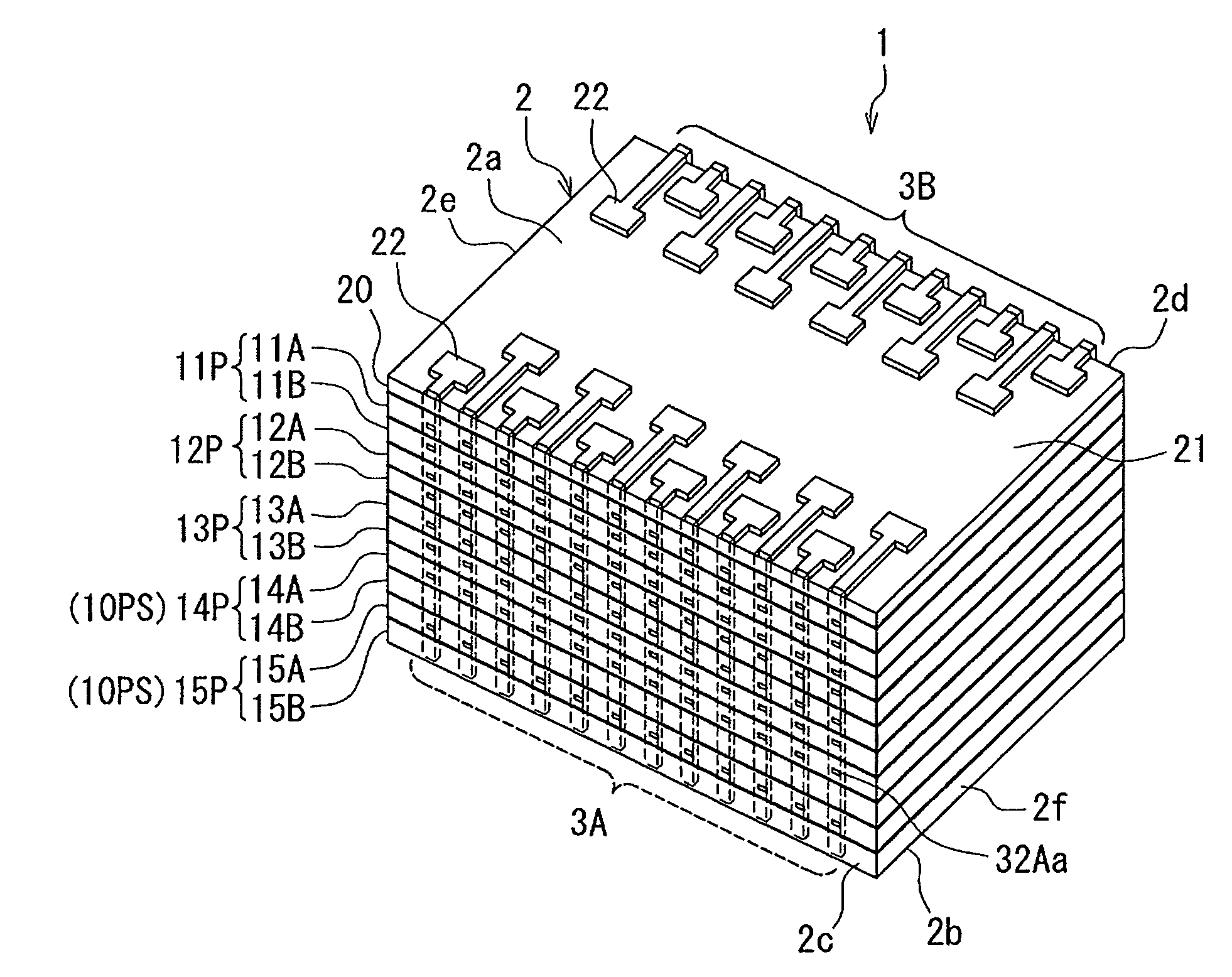
[0102]Embodiments of the present invention will now be described in detail with reference to the drawings. Reference is first made to FIG. 1 and FIG. 2 to describe the configuration of a layered chip package according to a first embodiment of the invention. Each of FIG. 1 and FIG. 2 is a perspective view of the layered chip package according to the present embodiment. FIG. 1 is drawn such that respective end faces of a plurality of first electrodes described later are visible. As shown in FIG. 1 and FIG. 2, the layered chip package 1 according to the present embodiment includes a main body 2 in the shape of a rectangular solid. The main body 2 has a top surface 2a, a bottom surface 2b, a first side surface 2c and a second side surface 2d facing toward opposite directions, and a third side surface 2e and a fourth side surface 2f facing toward opposite directions.

[0103]The layered chip package 1 further includes wiring disposed on at least one of the side surfaces of the main body 2. ...

second embodiment

[0228]A layered chip package 1 according to a second embodiment of the invention and its manufacturing method will now be described. Reference is now made to FIG. 37 to describe the configuration of the layered chip package 1 according to the present embodiment. FIG. 37 is a perspective view of the layered chip package 1 according to the present embodiment drawn such that the respective end faces 32Aa of the plurality of first electrodes 32A are visible.

[0229]The layered chip package 1 according to the present embodiment includes like the first embodiment, a main body 2 that is in the shape of a rectangular solid and that has a top surface 2a, a bottom surface 2b and first to fourth side surfaces 2c, 2d, 2e and 2f, and wiring 3 disposed on at least one of the side surfaces of the main body 2. In the example shown in FIG. 37, the layered chip package 1 includes first wiring 3A disposed on the first side surface 2c of the main body 2, and second wiring 3B disposed on the second side s...

third embodiment

[0246]A layered chip package 1 according to a third embodiment of the invention and its manufacturing method will now be described. Reference is now made to FIG. 41 to describe the configuration of the layered chip package 1 according to the present embodiment. FIG. 41 is a perspective view of the layered chip package 1 according to the present embodiment drawn such that the respective end faces 32Aa of the plurality of first electrodes 32A are visible.

[0247]The layered chip package 1 according to the present embodiment includes, like the first embodiment, a main body 2 that is in the shape of a rectangular solid and that has a top surface 2a, a bottom surface 2b and first to fourth side surfaces 2c, 2d, 2e and 2f, and wiring 3 disposed on at least one of the side surfaces of the main body 2. In the example shown in FIG. 41, the layered chip package 1 includes first wiring 3A disposed on the first side surface 2c of the main body 2, and second wiring 3B disposed on the second side s...


PUM


Abstract

A layered chip package has a main body including pairs of layer portions, and wiring disposed on a side surface of the main body. Each layer portion includes a semiconductor chip. The pairs of layer portions include at least one specific pair of layer portions including a first-type layer portion and a second-type layer portion. The first-type layer portion includes electrodes each connected to the semiconductor chip and each having an end face located at the side surface of the main body on which the wiring is disposed, whereas the second-type layer portion does not include such electrodes. A layered substructure formed of a stack of two substructures, each of which includes aligned preliminary layer portions, is used to fabricate a stack of a predetermined two or greater number of pairs of layer portions, and the main body is fabricated by stacking an additional first-type layer portion together with the stack, the number of the additional first-type layer portion being equal to the number of the specific pair(s) of layer portions included in the stack.

Description

BACKGROUND OF THE INVENTION[0001]1. Field of the Invention[0002]The present invention relates to a layered chip package including a plurality of chips stacked, and to a method of manufacturing the same.[0003]2. Description of the Related Art[0004]In recent years, a reduction in weight and an improvement in performance have been demanded of mobile devices typified by cellular phones and notebook personal computers. Accordingly, there has been a demand for higher integration of electronic components for use in mobile devices. Higher integration of electronic components has been demanded also for achieving an increase in capacity of semiconductor memory.[0005]As an example of highly integrated electronic components, a system-in-package (hereinafter referred to as SiP), especially an SiP utilizing a three-dimensional packaging technology for stacking a plurality of chips, has attracting attention in recent years. In the present application, a package including a plurality of chips stack...

Claims


Application Information

Patent Timeline
Patent Type & Authority Patents(United States)
IPC IPC(8): H01L21/00H01L23/48
CPCH01L24/24H01L24/25H01L24/82H01L24/94H01L24/96H01L25/0657H01L25/50H01L2924/07802H01L2924/10253H01L2224/48H01L24/48H01L2221/68359H01L2223/54426H01L2224/18H01L2224/49175H01L2224/4943H01L2225/06551H01L2924/01029H01L2924/01078H01L2924/01082H01L2924/30105H01L2924/30107H01L2924/01005H01L2924/01006H01L2924/01033H01L2924/014H01L2924/00H01L2924/181H01L2224/05554H01L2224/48463H01L2924/00014H01L2924/10161H01L24/49H01L2224/94H01L2224/73267H01L2224/32145H01L2224/023H01L2224/45099H01L2224/45015H01L2924/207H01L2224/03H01L2924/0001
Inventor SASAKI, YOSHITAKAITO, HIROYUKIHARADA, TATSUYAOKUZAWA, NOBUYUKISUEKI, SATORUIKEJIMA, HIROSHI
Owner HEADWAY TECH INC
Why Eureka
Try Eureka