

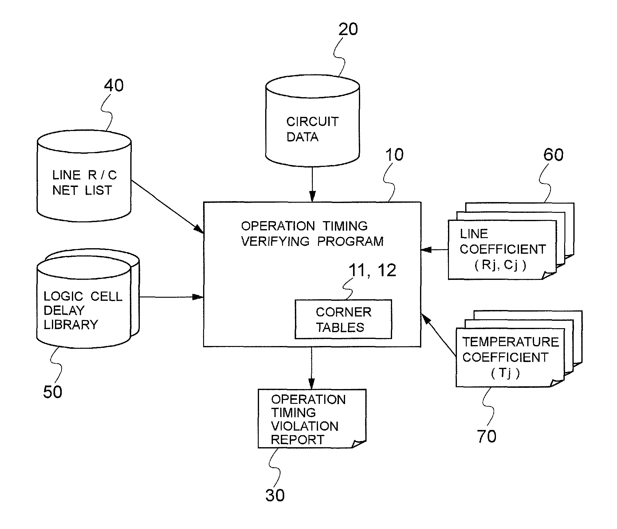
Operation timing verifying apparatus and program
a technology of operation timing and verification apparatus, applied in the direction of program control, instruments, computer aided design, etc., can solve the problems of increasing design time and cost for verifying operation timing, complicated analysis tools, etc., and achieve the effect of suppressing design time and cos
- Summary
- Abstract
- Description
- Claims
- Application Information
AI Technical Summary
Benefits of technology
Problems solved by technology
Method used
Image

Examples
Embodiment Construction
[0023]An embodiment of the present invention will be described in detail below with reference to the accompanying drawings.
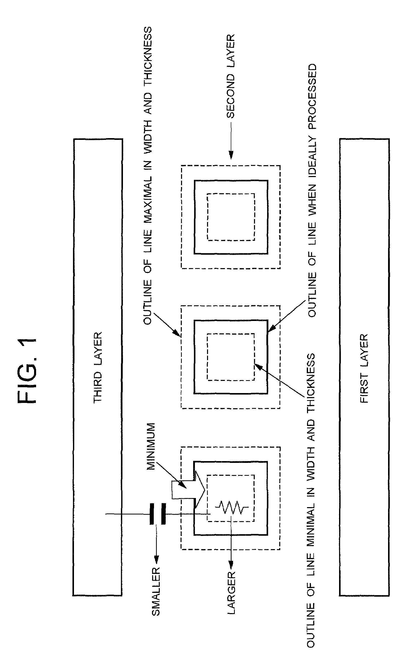
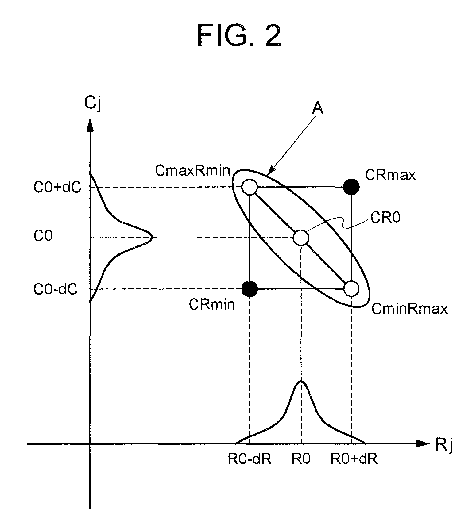
[0024]FIG. 1 illustrates a physical relationship between line capacitances and line resistances in a multi-layer structured semiconductor integrated circuit. The physical relationship is as follows. The condition for line capacitances becoming larger is that the distances of lines above, below, to the left, and to the right with respect to a line of a center second layer become smaller, namely, that the width and thickness of lines of the second layer become larger. However, under the condition that the width and thickness of lines of the second layer become larger, the line resistances of the second layer lines become smaller because their cross-section areas become larger. In contrast, the condition for line resistances becoming larger is that the width and thickness of the lines become smaller. However, under that condition, their line capacitances become sma...
PUM
 Abstract
Description
Claims
Application Information