Techniques for filtering systematic differences from wafer evaluation parameters

a technology of filtering and systematic differences, applied in the direction of testing circuits, instruments, digital computer details, etc., can solve the problems of visual, computationally and storage-allocation intensive, and all variation other than wafer level variation

Inactive Publication Date: 2011-08-02
MENTOR GRAPHICS CORP
View PDF3 Cites 5 Cited by
  • Summary
  • Abstract
  • Description
  • Claims
  • Application Information

AI Technical Summary

Problems solved by technology

For the above reasons, a total collection of measurement data in general, and a visual display of the measurement data values or parameters computed from the measurement data values more specifically, typically yields a poor result in that all of the variation other than the wafer level variation contributes to visual and numerical “noise” that masks the wafer-level variation in other variation.
Other systems that attempt to remove reticle level variation from wafer-level variation require generation of complex models that introduce error and are computationally and storage-allocation intensive.

Method used


Image

  • Techniques for filtering systematic differences from wafer evaluation parameters
  • Techniques for filtering systematic differences from wafer evaluation parameters
  • Techniques for filtering systematic differences from wafer evaluation parameters

Examples


Embodiment Construction

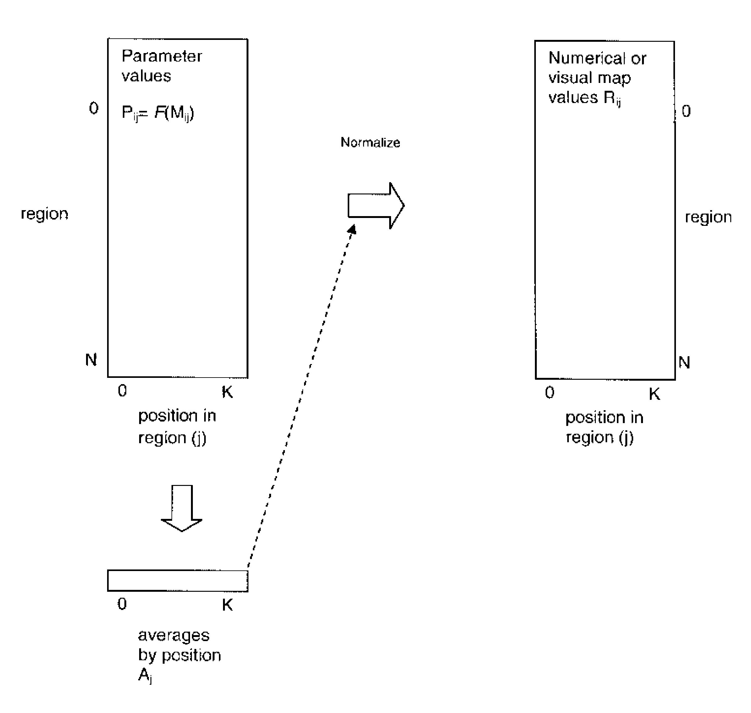
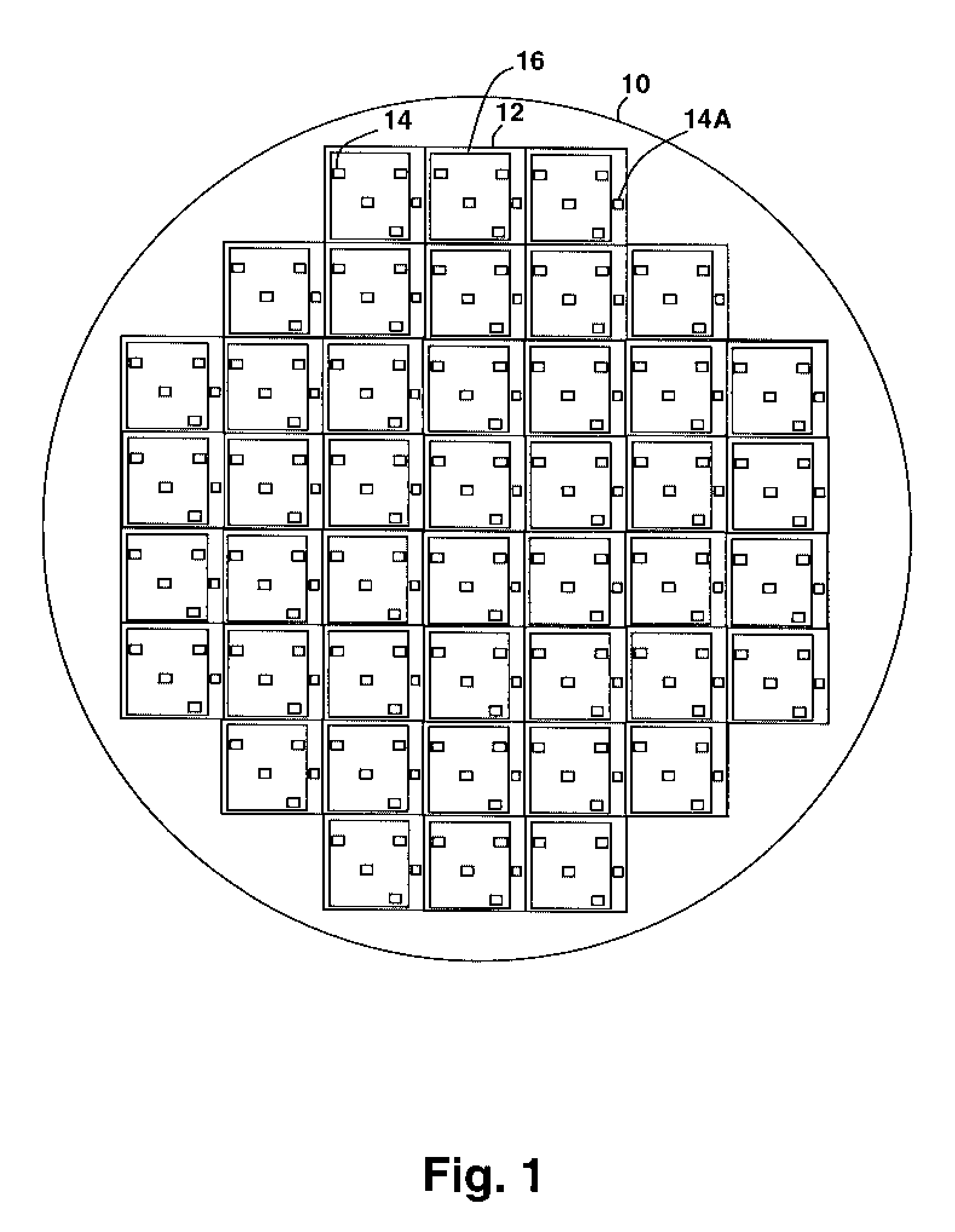
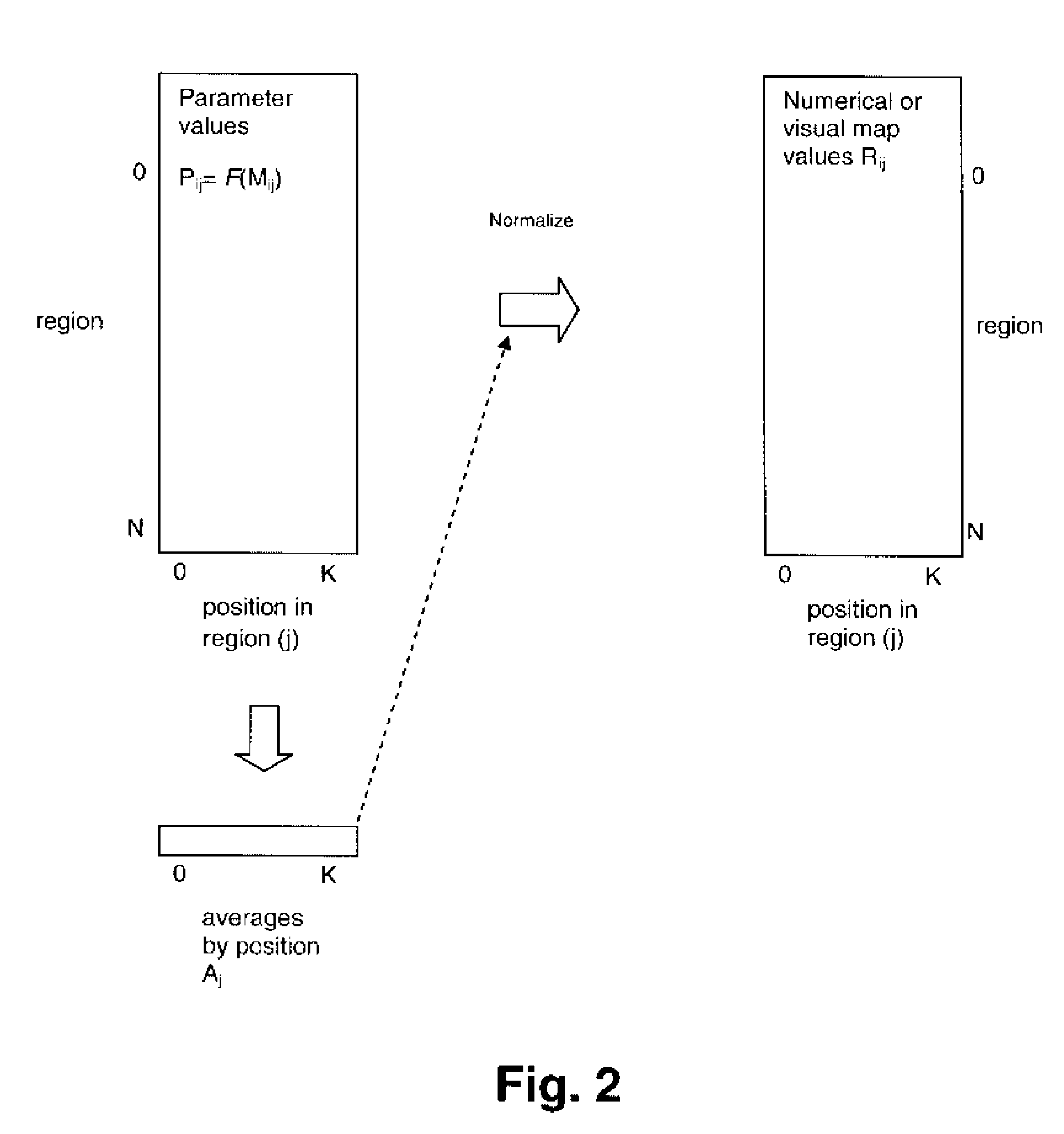
[0020]The present invention relates to a process characterization method and system that provide graphical display and / or numerical mapping of circuit measurements or parameters generated from circuit measurements across a wafer. To permit a higher resolution than is possible with display of data from individual disparate circuits and / or differing measurement value types, and to further enhance the visibility / resolution of the process variation display even when circuits are of the same type, the present invention uses a normalization procedure that permits mapping of measurement values from circuits having different design and / or differing measurement value types to a single parameter that is mapped across the wafer. Wafer-level process variation can then be viewed in the graphical display or numerical map by noting changes in the parameter. The graphical display may use color gradations, intensity (color or white / black brightness) levels and the like to show the value of the param...


PUM


Abstract

A method, system and computer program product for filtering systematic differences from wafer evaluation parameters provides an efficient visual display and numerical map technique for observing wafer-level process variation. Measurement data is gathered from electronic circuits at multiple positions within multiple regions on one or more wafers and parameters are computed from the measurement data, which may be the measurement data values themselves. The set of parameters is filtered for expected systematic variation by computing a set of normalization values from the set of parameters and normalizing the data according to the normalization values. The normalized parameter set is then either presented in a visual display, e.g., by color mapping, or arranged in a numerical map of parameter value by location.

Description

BACKGROUND OF THE INVENTION[0001]1. Field of the Invention[0002]The present invention is related to wafer characterization methods and measurements, and more particularly to a method, system and computer program product for isolating circuit or block level systematic differences from wafer measurement data and / or evaluation parameters computed therefrom.[0003]2. Description of Related Art[0004]Study of wafer-level measurement data variation, and / or evaluation parameters computed from measurement data, provides insight into several process mechanisms that cause significant differences in operation of circuits fabricated on a wafer. In particular systematic variations in etching and anneal processes across the wafer are typically independent of the systematic variations due to imaging processes, which cause variation on a particular basis. Characteristics of the wafer itself also may cause variation across the wafer. It is desirable to visualize and also to numerically characterize th...

Claims


Application Information

Patent Timeline
Patent Type & Authority Patents(United States)
IPC IPC(8): G01R31/00
CPCG01R31/2894G01R31/2831
Inventor GATTIKER, ANNE ELIZABETH
Owner MENTOR GRAPHICS CORP
Why Eureka
Try Eureka