Defect management for a semiconductor memory system

a technology of memory system and defect management, which is applied in the field of defect management of semiconductor memory system, can solve the problems of increasing memory data error rate, increasing the amount of memory capacity overhead, and increasing the number of errors capabl

Inactive Publication Date: 2011-08-09
HEWLETT-PACKARD ENTERPRISE DEV LP
View PDF33 Cites 13 Cited by
  • Summary
  • Abstract
  • Description
  • Claims
  • Application Information

AI Technical Summary

Problems solved by technology

However, increasing memory data error rates often accompany these advancements.
More specifically, both “hard errors” (permanent defects in a memory device, such as one or more defective memory cells) and “soft errors” (data errors of a temporary nature, such as inversion of data held within one or more memory cells) tend to become more prevalent with each new technology generation.
Typically, the more EDC data being utilized, the higher the number of errors capable of being detected and corrected, but also the higher the amount of memory capacity overhead incurred.
However, similar to the use of EDC, the use of spare devices also increases the cost and memory overhead associated with the memory system.
Even with these advanced memory protection mechanisms, further memory technological advances often involve attendant increases in hard and soft error rates, thus reducing device reliability.
Also, new memory device generations often introduce new memory failure modes.
Thus, such advances in memory technology may have the unintended effect of reducing the effectiveness of the EDC and related schemes currently employed in computer memory systems.

Method used


Image

  • Defect management for a semiconductor memory system
  • Defect management for a semiconductor memory system
  • Defect management for a semiconductor memory system

Examples


Embodiment Construction

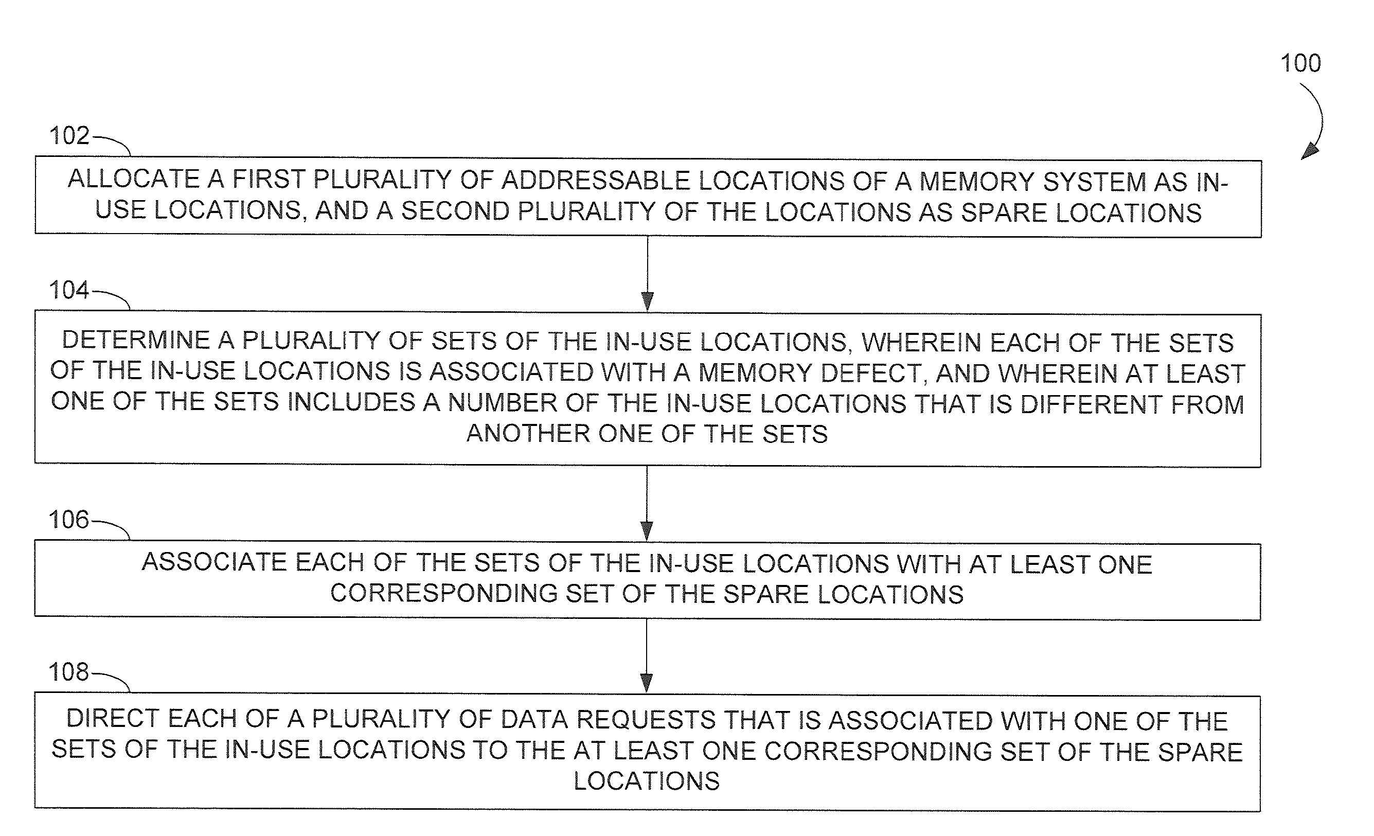
[0013]FIG. 1 provides a flow diagram of a method 100 according to an embodiment of the invention for managing memory defects in a semiconductor memory system. A memory defect may be any defect of the semiconductor memory system that causes hard or soft errors affecting data stored within the memory system. In the method 100, addressable locations within the memory system are allocated into a first plurality of locations as in-use locations, and a second plurality of locations as spare locations (operation 102). A plurality of sets of the in-use locations, wherein each of the sets of the in-use locations is associated with a memory defect, is determined (operation 104). At least one of the sets includes a different number of the in-use locations than another one of the sets. Each of the sets of the in-use locations is then associated with at least one corresponding set of the spare locations (operation 106). Each of a plurality of data requests that is associated with one of the sets...


PUM


Abstract

A method is provided for managing defects in a semiconductor memory system having a plurality of addressable locations. In the method, a first plurality of the addressable locations is allocated as in-use locations, and a second plurality of the addressable locations is allocated as spare locations. A plurality of sets of the in-use locations, wherein each of the sets is associated with a memory defect, is determined. At least one of the sets includes a different number of in-use locations than another of the sets. Each of the sets of the in-use locations is associated with at least one corresponding set of the spare locations. Each of a plurality of data requests that is associated with one of the sets of the in-use locations is directed to the at least one corresponding set of the spare locations.

Description

BACKGROUND OF THE INVENTION[0001]A vital component of virtually all computer systems is a semiconductor or solid-state memory system. The memory system often holds both the programming instructions for a processor of the computer system, as well as the data upon which those instructions are executed. In one example, the memory system may include one or more dual in-line memory modules (DIMMs), with each DIMM carrying multiple dynamic random access memory (DRAM) integrated circuits (ICs). Other memory technologies, such as static random access memories (SRAMs), and various memory organizational structures, such as single in-line memory modules (SIMMs), are also employed in a variety of computer systems. In addition, one or more processors may be coupled with the memory modules through a memory controller, which translates data requests from the processor into accesses to the data held in the memory modules. In addition, many systems provide one or more levels of cache memory residing...

Claims


Application Information

Patent Timeline
Patent Type & Authority Patents(United States)
IPC IPC(8): G06F11/00
CPCG06F12/0246
Inventor NAGARAJ, DHEEMANTHTHAYER, LARRY J.
Owner HEWLETT-PACKARD ENTERPRISE DEV LP
Why Eureka
Try Eureka