Semiconductor light emitting device

a technology of light-emitting devices and semiconductors, which is applied in the direction of semiconductor devices, basic electric elements, electrical equipment, etc., can solve the problems of reduced luminous efficiency, limited light extraction, and caused light loss, and achieve high luminous efficiency

Active Publication Date: 2011-08-30
SAMSUNG ELECTRONICS CO LTD
View PDF14 Cites 439 Cited by
  • Summary
  • Abstract
  • Description
  • Claims
  • Application Information

AI Technical Summary

Benefits of technology

[0021]Further, another object of the present invention is to provide a semiconductor light emitting device with high luminous efficiency.

Problems solved by technology

As a result, light extraction is limited, light loss is caused due to optical absorption, and luminous efficiency is reduced.
The horizontal and vertical semiconductor light emitting devices, which are described with reference to FIGS. 1 and 2, reduce the light emitting area to thereby reduce the luminous efficiency, limit the light extraction, cause the light loss due to the optical absorption, and reduce the luminous efficiency.

Method used


Image

  • Semiconductor light emitting device
  • Semiconductor light emitting device
  • Semiconductor light emitting device

Examples


Embodiment Construction

[0042]Hereinafter, embodiments of the present invention for a semiconductor light emitting device will be described in detail with reference to the accompanying drawings. The following embodiments are provided as examples to fully convey the spirit of the invention to those skilled in the art. Therefore, the present invention should not be construed as limited to the embodiments set forth herein and may be embodied in different forms and. And, the size and the thickness of an apparatus may be overdrawn in the drawings for the convenience of explanation. The same component is represented by the same reference numeral hereinafter.

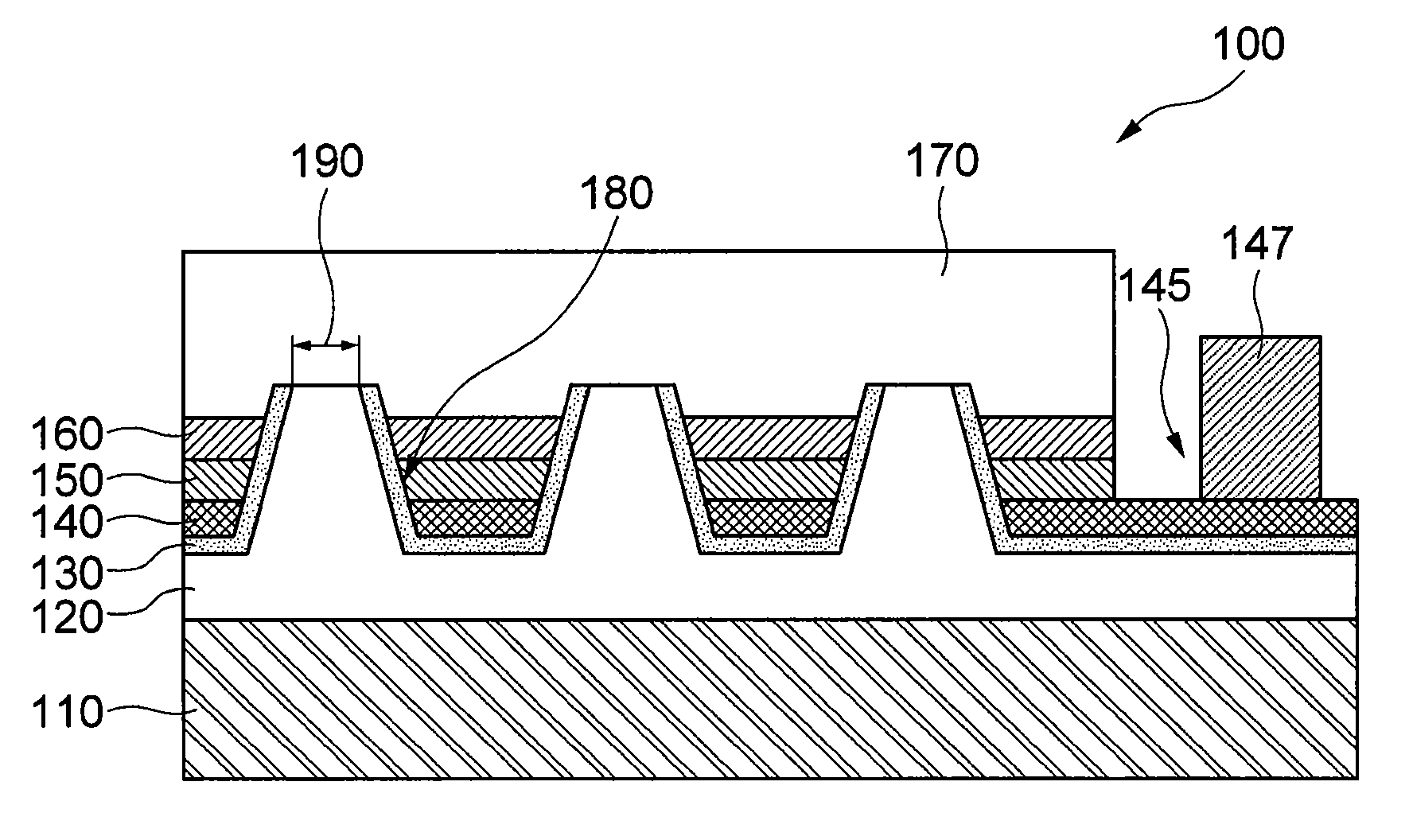
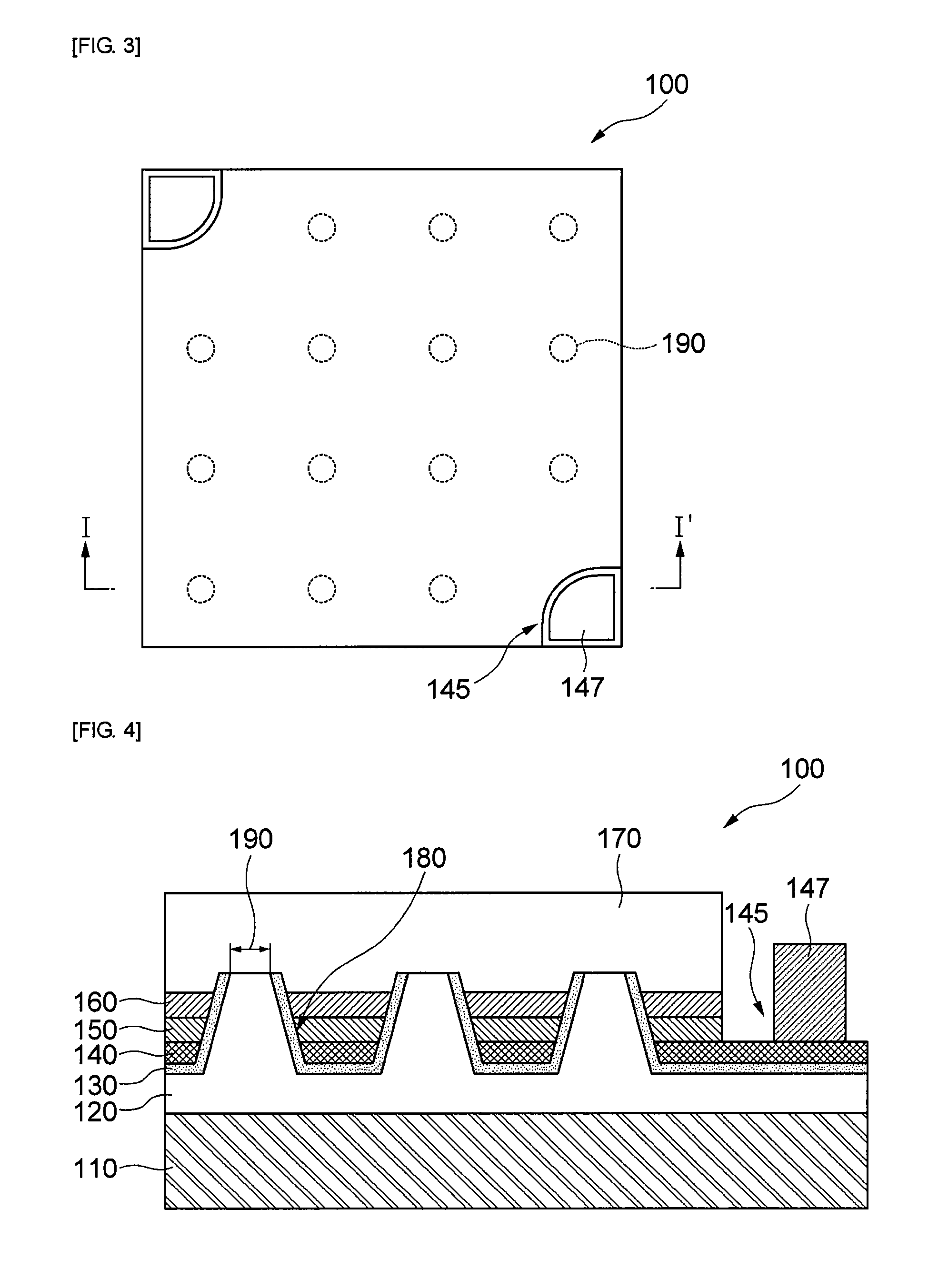
[0043]FIGS. 3 and 4 are a plane-view and a cross-sectional view illustrating a semiconductor light emitting device in accordance with one embodiment of the present invention. At this time, FIG. 4 is a cross-sectional view taken along a line I-I′ shown in FIG. 3.

[0044]Referring to FIGS. 3 and 4, a semiconductor light emitting device 100 in accordance with one ...


PUM


Abstract

The present invention provides a semiconductor light emitting device including a conductive substrate, a first electrode layer, an insulating layer, a second electrode layer, a second semiconductor layer, an active layer, and a first semiconductor layer which are sequentially stacked, wherein an area where the first electrode layer and the first semiconductor layer are in contact with each other is 3 to 13% of an area of the semiconductor light emitting device.

Description

CROSS-REFERENCE TO RELATED APPLICATIONS[0001]This application claims the benefit of Korean Patent Application No. 10-2008-0103671 filed with the Korea Intellectual Property Office on Oct. 22, 2008, the disclosure of which is incorporated herein by reference.BACKGROUND OF THE INVENTION[0002]1. Field of the Invention[0003]The present invention relates to a semiconductor light emitting device; and, more particularly, to a semiconductor light emitting device capable of performing an operation at a high current and improving luminous efficiency by changing an arrangement structure of electrodes.[0004]2. Description of the Related Art[0005]Semiconductor light emitting devices contain materials emitting light inside. For example, LEDs (Light Emitting Diodes) are devices that use diodes, to which semiconductors are bonded, convert energy generated by recombination of electrons and holes into light, and emit the light. The semiconductor light emitting devices are being widely used as lightin...

Claims


Application Information

Patent Timeline
Patent Type & Authority Patents(United States)
IPC IPC(8): H01L33/00
CPCH01L33/08H01L33/40H01L33/382H01L33/20H01L33/22H01L33/38H01L2224/48091H01L2224/48247H01L2933/0016H01L2924/00014H01L33/0093H01L33/0075H01L33/405H01L33/42
Inventor CHOI, PUN JAEKIM, YU SEUNGLEE, JIN BOCK
Owner SAMSUNG ELECTRONICS CO LTD
Why Eureka
Try Eureka