Display substrate, method for manufacturing the same, and display panel having the same

a technology of display substrate and manufacturing method, which is applied in the field of display substrate, a method for manufacturing display substrate, and a display panel having the same, can solve the problems of reducing the aperture ratio of the lcd panel and the luminance decrease, and achieves the effect of increasing the light reflection efficiency and enhancing the external visibility

Inactive Publication Date: 2011-08-30
SAMSUNG DISPLAY CO LTD
View PDF10 Cites 0 Cited by
  • Summary
  • Abstract
  • Description
  • Claims
  • Application Information

AI Technical Summary

Benefits of technology

[0008]Example embodiments of the present invention may provide a display substrate capable of enhancing light reflection efficiency. Also, embodiments of the present invention provide a method for manufacturing the display substrate and a display panel having the display substrate.
[0014]According to one or more embodiments—the display substrate, the method for manufacturing the display substrate, and the display panel having the display substrate—the first and second sensor drain electrodes and a dummy drain electrode have an embossed shape, and thus external visibility may be enhanced by increased light reflection efficiency.

Problems solved by technology

When the sensor electrode part is formed in the unit pixel, however, an aperture ratio of the LCD panel is decreased by the size of the sensor electrode part, which causes a decrease in luminance.

Method used


Image

  • Display substrate, method for manufacturing the same, and display panel having the same
  • Display substrate, method for manufacturing the same, and display panel having the same
  • Display substrate, method for manufacturing the same, and display panel having the same

Examples


example one

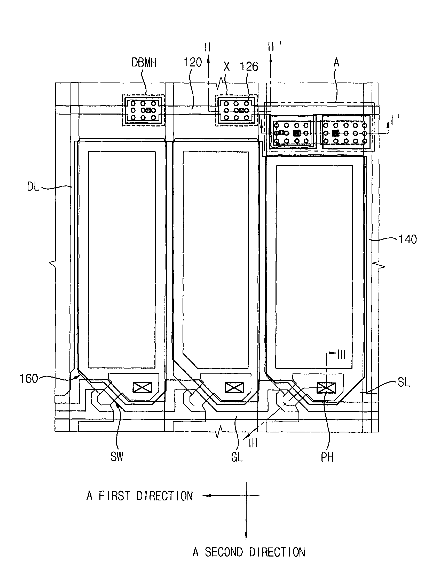
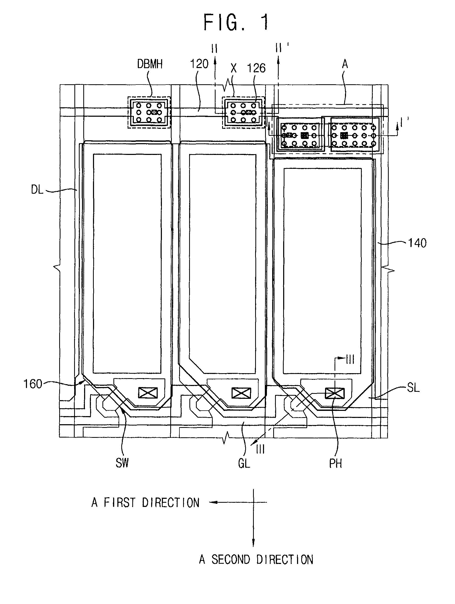
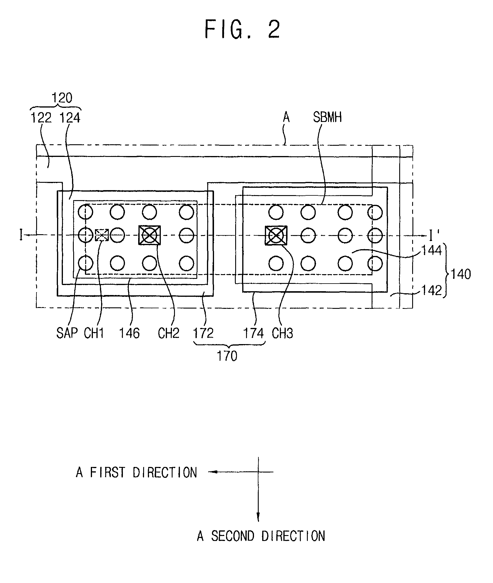
[0040]FIG. 1 is a plan view illustrating a part of a display panel according to an embodiment; FIG. 2 is a plan view magnifying a sensor part A in FIG. 1; and FIG. 3 is a cross-sectional view taken along a line I-I′ of a sensor part A in FIG. 1 in accordance with one or more embodiments.

[0041]Referring to FIGS. 1 through 3, the display panel according to an embodiment includes a display substrate 100, a counter substrate 200, and a liquid crystal layer 10; and displays an image to the exterior. The display substrate 100 includes pixel electrodes 160 disposed as a matrix forming, thin-film transistors (TFTs) SW electrically connected to the pixel electrodes 160, and gate lines GL and data lines DL electrically connected to the TFTs SW. The plurality of gate lines GL and data lines DL are formed in directions that cross each other, and define a plurality of unit regions on the display substrate 100. A part of the unit regions have a sensor part A sensing a position of pressure from th...

example two

[0072]FIG. 10 is a plan view illustrating a part of a display panel according to another embodiment; FIG. 11 is an enlarged plan view illustrating a sensor part B in FIG. 10; and FIG. 12 is a cross-sectional view taken along a line I-I′ of a sensor part B in FIG. 10 in accordance with one or more embodiments. A display substrate 300 is substantially the same as the display panel described in FIG. 1 except that a common electrode 163 is formed on a display substrate 300. Thus, the same reference numerals are used for the same elements and repeated descriptions will be omitted. FIG. 13 is a cross-sectional view taken along a line II-II′ of a dummy part Y in FIG. 10; and FIG. 14 is a cross-sectional view taken along a line III-III′ of a transistor SW in FIG. 10 in accordance with one or more embodiments.

[0073]Referring to FIGS. 10 through 14, the display substrate 300 includes pixel electrodes 160 disposed as a matrix shape, TFTs SW electrically connected to the pixel electrodes 160, g...

example three

[0093]FIG. 17 is a plan view illustrating a part of a display panel according to another embodiment; FIG. 18 is an enlarged plan view illustrating a sensor part C in FIG. 17; FIG. 19 is a cross-sectional view taken along a line I-I′ of a sensor part C in FIG. 17; and FIG. 20 is a cross-sectional view taken along a line II-II′ of a dummy part Z in FIG. 17 in accordance with one or more embodiments. A display substrate 500 is substantially the same as the display panel described in FIG. 10 except that a common electrode 163 is formed on a display substrate 500, and a first sensor gate electrode 524, a second gate electrode 525 and a dummy gate electrode 526 have a plurality of island-type sub-gate members. Thus, the same reference numerals are used for the same elements and repeated descriptions will be omitted.

[0094]Referring to FIGS. 17 to 20, the display substrate 500 includes a first base substrate 110, a gate line GL, a storage line SL, a first sensor line 520, a gate insulation ...


PUM

PropertyMeasurementUnit
shapeaaaaaaaaaa
areaaaaaaaaaaa
external pressureaaaaaaaaaa

Abstract

A gate line and a data line are formed on a base substrate. A first sensor line is parallel with the gate line. A sensor gate electrode is extended from the first sensor line. A sensor active pattern having a plurality of island-type sub-active members is formed on the first sensor gate electrode. A second sensor line is parallel with the data line. A first sensor drain electrode is extended from the second sensor line at the sensor active pattern. A second sensor drain electrode corresponding to the first sensor gate electrode is formed on the sensor active pattern. A pixel electrode is electrically connected to the gate line and the data line. A sensor electrode part electrically connects the first and second sensor drain electrodes spaced apart from the pixel electrode. Light is reflected by the first and second sensor drain electrodes, which have an embossed shape.

Description

CROSS REFERENCE TO RELATED APPLICATIONS[0001]This application claims priority under 35 U.S.C. §119 to Korean Patent Application No. 2008-120844, filed on Dec. 2, 2008 in the Korean Intellectual Property Office (KIPO), the contents of which are herein incorporated by reference in their entirety.BACKGROUND[0002]1. Technical Field[0003]The present invention generally relates to a display substrate, a method for manufacturing the display substrate, and a display panel having the same. More particularly, the present invention relates to a display substrate that may provide enhanced display quality, a method for manufacturing the display substrate, and a display panel having the same.[0004]2. Related Art[0005]Liquid crystal display (LCD) devices are known to have characteristics—such as light weight, lower power consumption, and lower driving voltage—in comparison with other types of display apparatuses, rendering them useful, for example, in monitors, notebook computers, and cellular pho...

Claims


Application Information

Patent Timeline
Patent Type & Authority Patents(United States)
IPC IPC(8): G02F1/1335G02F1/1343G02F1/13
CPCG02F1/13338G06F3/0412G02F1/133345G02F1/133555G02F1/134363G02F1/136286G02F2001/134372G02F2201/40G02F2201/50G06F3/047G02F1/134372G02F1/133G02F1/136
Inventor JEONG, YOUN-HAKOH, KEUN-CHANHAM, YEON-SIKSEONG, DONG-GIKIM, KANG-WOOJEON, YEON-MUNLEE, HEE-HWAN
Owner SAMSUNG DISPLAY CO LTD
Why Eureka
Try Eureka