Substrate surface micro-processing method, composite substrate and LED epitaxial wafer

A substrate surface and composite substrate technology, applied in the direction of electrical components, circuits, semiconductor devices, etc., to achieve the effects of increasing surface area, improving light reflection efficiency, and increasing external quantum efficiency

Active Publication Date: 2021-10-29
广东中图半导体科技股份有限公司
View PDF7 Cites 0 Cited by
  • Summary
  • Abstract
  • Description
  • Claims
  • Application Information

AI Technical Summary

Problems solved by technology

[0003] The size of a single pattern on a patterned substrate is generally at or below the micron level. At present, there are few methods that can only roughen the surface of the pattern without affecting the surface at other positions.

Method used


Image

  • Substrate surface micro-processing method, composite substrate and LED epitaxial wafer
  • Substrate surface micro-processing method, composite substrate and LED epitaxial wafer
  • Substrate surface micro-processing method, composite substrate and LED epitaxial wafer

Examples


Embodiment Construction

[0039] The present invention will be further described in detail below in conjunction with the accompanying drawings and embodiments. It should be understood that the specific embodiments described here are only used to explain the present invention, but not to limit the present invention. In addition, it should be noted that, for the convenience of description, only some structures related to the present invention are shown in the drawings but not all structures.

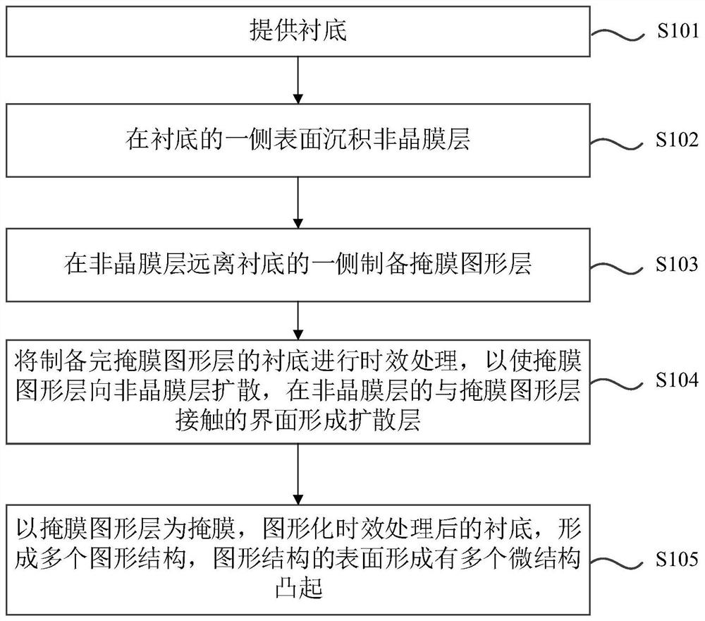
[0040] figure 1 The flow chart of a micro-processing method for the substrate surface provided by the embodiment of the present invention, this embodiment is applicable to the preparation of the surface microstructure of the sapphire substrate, and further, the prepared sapphire substrate can be used to prepare the LED Epiwafer. like figure 1 As shown, the microprocessing method includes:

[0041] S101, providing a substrate.

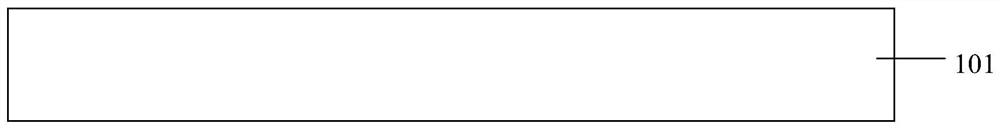
[0042] like figure 2 As shown, the substrate 101 can be a planar single crystal s...


PUM

PropertyMeasurementUnit
corrosion rateaaaaaaaaaa
surface roughnessaaaaaaaaaa
refractive indexaaaaaaaaaa

Abstract

The embodiment of the invention discloses a substrate surface micro-processing method, a composite substrate and an LED epitaxial wafer, and the micro-processing method comprises the steps that: a substrate is provided, an amorphous film layer is deposited on surface of one side of the substrate, a mask pattern layer is prepared on the side, away from the substrate, of the amorphous film layer, and aging treatment is carried out on the substrate with the prepared mask pattern layer. The mask pattern layer is made to diffuse towards the amorphous film layer, a diffusion layer is formed on the interface, making contact with the mask pattern layer, of the amorphous film layer, the substrate obtained after aging treatment is further patterned, a plurality of pattern structures are formed, and due to the fact that the diffusion layer and the amorphous film layer are different in density, a plurality of microstructure protrusions are formed on the surfaces of the pattern structures during etching. According to the micro-processing method provided by the embodiment of the invention, the surface of the patterned structure of the patterned substrate can be coarsened and controlled without influencing the surfaces of other positions, the surface area of the patterned structure is increased, the light reflection efficiency of the patterned substrate is improved, and the external quantum efficiency of the LED epitaxial wafer can be further improved.

Description

technical field [0001] The embodiments of the present invention relate to the technical field of surface treatment, in particular to a method for micro-processing the surface of a substrate, a composite substrate and an LED epitaxial wafer. Background technique [0002] Patterned substrate is currently the most important substrate material for GaN LED epitaxial growth. The microstructure and optical parameters of its surface pattern have a great influence on the quality of the epitaxial wafer, such as patterning with the same size and different surface roughness. After the substrate undergoes the same epitaxial process, there is a big difference in its epitaxial comprehensive quality. [0003] The size of a single pattern on a patterned substrate is generally at or below the micron level. At present, there are few methods that can only roughen the surface of the pattern without affecting the surface at other positions. Contents of the invention [0004] The embodiment of ...

Claims


Application Information

Patent Timeline
Patent Type & Authority Applications(China)
IPC IPC(8): H01L33/00H01L33/22
CPCH01L33/22H01L33/005
Inventor 曾广艺
Owner 广东中图半导体科技股份有限公司
Why Eureka
Try Eureka