A high reflectivity vertical structure light-emitting diode chip and its preparation method

A light-emitting diode and vertical structure technology, applied in the direction of electrical components, circuits, semiconductor devices, etc., can solve the problems of not meeting the expectations of cost performance, achieve good ohmic contact performance, reduce loss, and increase the effect of light reflection efficiency

Inactive Publication Date: 2018-03-23
INST OF SEMICONDUCTORS - CHINESE ACAD OF SCI
View PDF5 Cites 0 Cited by
  • Summary
  • Abstract
  • Description
  • Claims
  • Application Information

AI Technical Summary

Problems solved by technology

However, the current speed of efficiency improvement and cost reduction is far from meeting the market's expectations for LED cost performance

Method used


Image

  • A high reflectivity vertical structure light-emitting diode chip and its preparation method
  • A high reflectivity vertical structure light-emitting diode chip and its preparation method
  • A high reflectivity vertical structure light-emitting diode chip and its preparation method

Examples


preparation example Construction

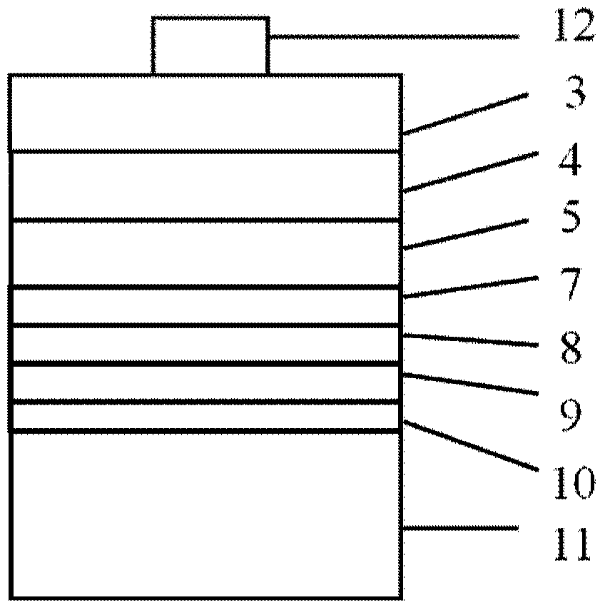
[0042] based on figure 1 The structure diagram of the vertical light-emitting diode chip with high reflectivity shown in the present invention also provides a preparation method of a vertical light-emitting diode chip with high reflectivity, comprising the following steps:

[0043]Step 1: select a substrate, and epitaxially grow a buffer layer, an N-type layer, a multi-quantum well layer and a P-type layer on the substrate in sequence to form an epitaxial layer;

[0044] Step 2: performing photolithographic etching on the epitaxial layer, and depositing a passivation layer;

[0045] Step 3: sequentially vapor-deposit an ohmic contact layer, a metal reflective layer, a barrier layer and an anti-oxidation layer on the passivation layer, and anneal to form a highly reflective P-type ohmic contact layer;

[0046] Step 4: Electroplating on the highly reflective P-type ohmic contact layer to make a heat dissipation substrate;

[0047] Step 5: removing the substrate and buffer laye...

Embodiment 1

[0053] The preparation method of the light-emitting diode chip with vertical structure in Example 1 of the present invention is as follows:

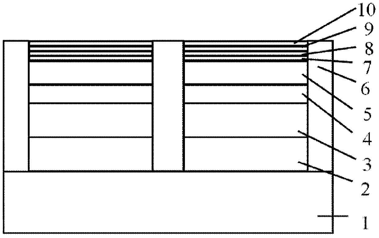
[0054] 1) Epitaxy on the sapphire substrate 1, grow buffer layer 2, N-type layer 3, multi-quantum well layer 4, P-type layer 5 in sequence, and then the wafer is heated at 700 ° C, N 2 Annealing under atmosphere for 20 minutes;

[0055] 2) Through photolithography and dry etching until the substrate, the etching depth is about 7 μm, and the platform is independent;

[0056] 3) Depositing a 2 μm passivation layer 6 to protect the etched sidewall, and the passivation layer 6 is made of silicon dioxide;

[0057] 4) Evaporating a highly reflective P-type ohmic contact layer, including: ohmic contact layer 7 (Ni), reflective layer 8 (Ag), barrier layer 9 (Ni) and anti-oxidation layer 10 (Au);

[0058] 5) 500°C in O 2 Annealing the highly reflective P-type ohmic contact layer under atmosphere;

[0059] 6) Electroplating metal Ni substrate ...

Embodiment 2

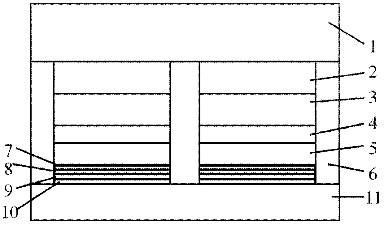
[0065] A buffer layer 2 , a GaN N-type layer 3 , a multi-quantum well layer 4 and a GaN P-type layer 5 are grown on a sapphire substrate 1 . Photolithography to form patterns, dry etching to the sapphire substrate, etching the side to deposit a passivation layer 6, and vapor-depositing a highly reflective P-type ohmic contact layer (ohmic contact layer 7, reflective layer 8, barrier layer 9 and anti-oxidation layer 10 ) and annealing, electroplating the metal substrate 11, removing the sapphire substrate 1, removing the buffer layer 2, evaporating the metal layer 12 to make an N electrode, and finally dicing, testing, and sorting the wafer.


PUM


Abstract

The invention discloses a high-reflectiveness vertical structure light emitting diode chip. The chip is of a single-electrode structure and comprises a radiating substrate, a high-reflectiveness P-type ohmic contact layer and an epitaxial layer from bottom to top in sequence; the high-reflectiveness P-type ohmic contact layer comprises an anti-oxidation layer, a barrier layer, a metal reflection layer and an ohmic contact layer from bottom to top in sequence; the epitaxial layer consists of a P type layer, a multiple quantum well layer and an N type layer from bottom to top in sequence; an N electrode is manufactured on the N type layer. The invention also discloses a preparation method of the high-reflectiveness vertical structure light emitting diode chip. According to the manufactured chip, light output can be effectively increased, the radiating capacity of the chip is improved, stable light output power is provided, and application of high luminous efficiency is realized.

Description

technical field [0001] The invention relates to the design of a semiconductor light-emitting device, in particular to a vertical-structure light-emitting diode chip with high reflectivity P-type ohmic contact and a preparation method thereof. Background technique [0002] New semiconductor light sources represented by GaN-based light-emitting diodes (LEDs) are called fourth-generation lighting sources or green light sources. Compared with traditional light sources, it has attracted much attention because of its advantages such as high luminous efficiency, energy saving, environmental protection, and long life. Some developed countries and regions have formulated semiconductor lighting development plans in order to completely replace traditional light sources with LED light sources and trigger a new revolution in the lighting industry. With the continuous improvement of LED lighting technology and the continuous advancement of LED industrialization, it is the general trend f...

Claims


Application Information

Patent Timeline
Patent Type & Authority Patents(China)
IPC IPC(8): H01L33/40H01L33/64H01L33/00
CPCH01L33/0075H01L33/405H01L33/641H01L33/642H01L2933/0016H01L2933/0066H01L2933/0075
Inventor 赵桂娟汪连山杨少延刘贵鹏魏鸿源焦春美刘祥林朱勤生王占国
Owner INST OF SEMICONDUCTORS - CHINESE ACAD OF SCI
Why Eureka
Try Eureka