Light-emitting diode, electronic device and fabrication method

A technology of light-emitting diodes and manufacturing methods, which can be applied to circuits, electrical components, semiconductor devices, etc., and can solve problems such as low LED lumen efficiency

Inactive Publication Date: 2012-01-25
瑞峰(张家港)光伏科技有限公司
View PDF3 Cites 3 Cited by
  • Summary
  • Abstract
  • Description
  • Claims
  • Application Information

AI Technical Summary

Problems solved by technology

[0004] The purpose of the present invention is to solve the problem of low lumen efficiency of LEDs in the prior art. Embodiments of the present invention provide a light-emitting diode, electronic equipment and a manufacturing method. The substrate of the light-emitting diode is sequentially provided with a The semiconductor layer, the multi-quantum well structure and the second conductivity type semiconductor laye...

Method used


Image

  • Light-emitting diode, electronic device and fabrication method
  • Light-emitting diode, electronic device and fabrication method
  • Light-emitting diode, electronic device and fabrication method

Examples


Embodiment Construction

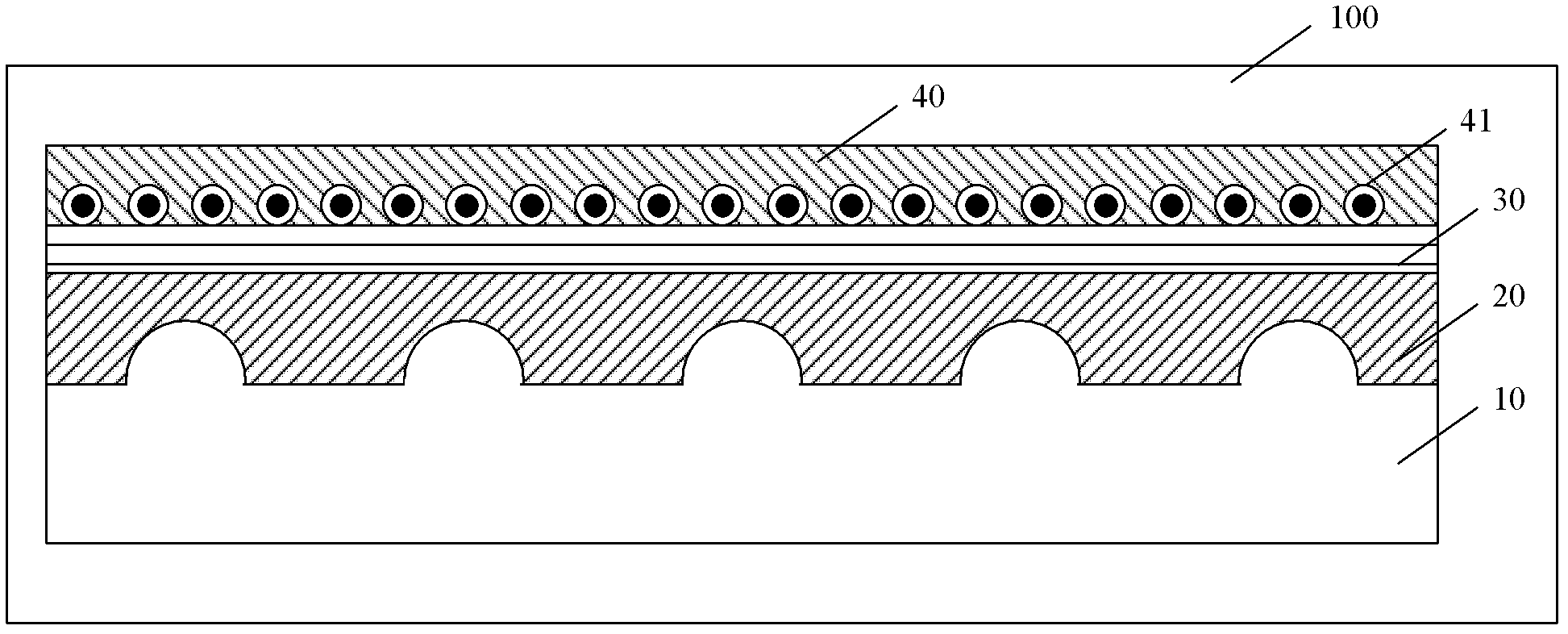
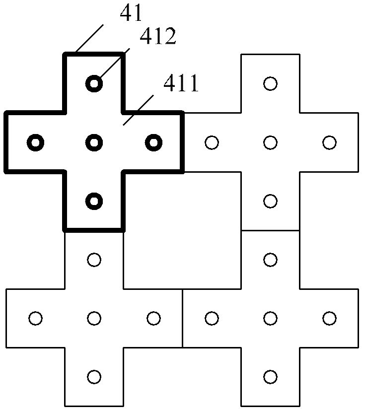
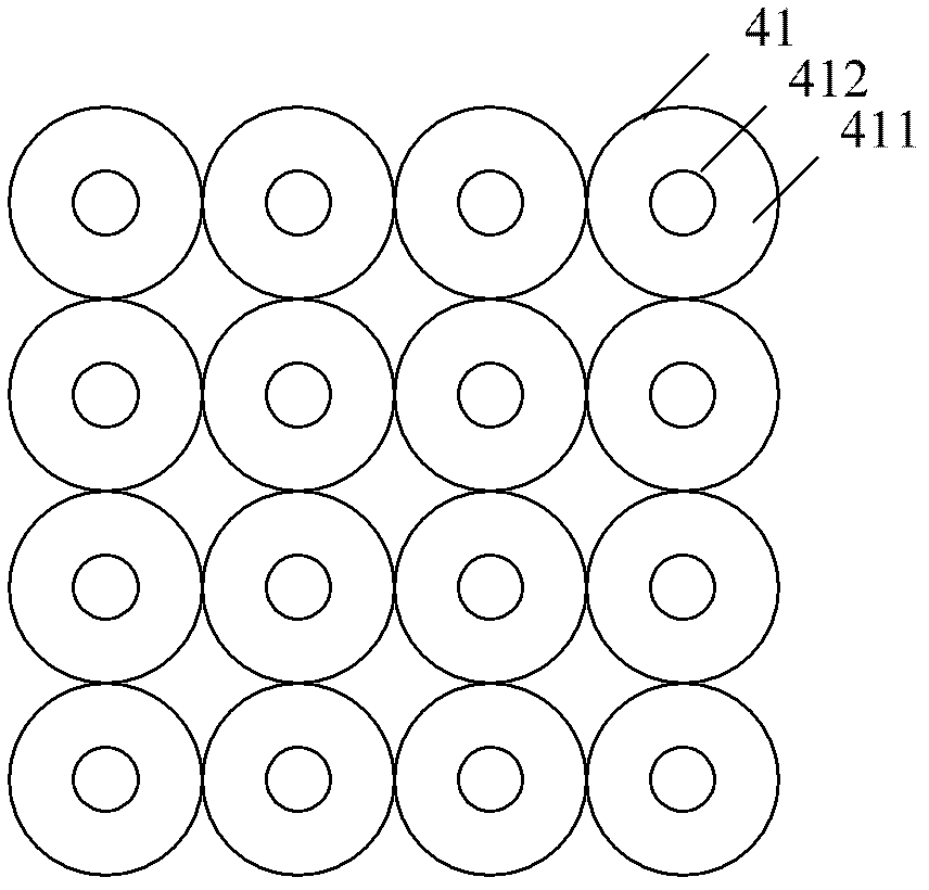
[0037] figure 1 It is a schematic structural diagram of an embodiment of a light emitting diode 100 according to the present invention. The substrate 10 of the light emitting diode 100 is sequentially provided with a first conductivity type semiconductor layer 20 , a multi-quantum well structure 30 and a second conductivity type semiconductor layer 40 . The position adjacent to the MQW 30 in the type semiconductor layer 40 is embedded with a plurality of metal nanogroups 41 with gaps between them. The nanoparticle group 41 has a dielectric outer layer and a metal nanoparticle core wrapped by the outer layer. The gaps of the particle group 41 are filled with the second conductivity type semiconductor material.

[0038] As a preferred solution in this embodiment, the first conductivity type semiconductor layer is an n-type semiconductor layer, the second conductivity type semiconductor layer is a p-type semiconductor layer, and the material of the n-type semiconductor layer can ...


PUM

PropertyMeasurementUnit
Thicknessaaaaaaaaaa

Abstract

The invention discloses a light-emitting diode, an electronic device and a fabrication method, which solve the problem of the prior art that the luminous efficiency of the LED (light-emitting diode) is still low. A first conduction type semiconductor layer, a multi-quantum well structure and a second conduction type semiconductor layer are sequentially arranged on a substrate of the light-emitting diode, wherein a plurality of nanoparticle sets which are spaced from one another are embedded at a position in the second conduction type semiconductor layer, which is close to the multi-quantum well structure, each nanoparticle set is provided with a dielectric outer surface layer and a metal nanoparticle core wrapped by the outer surface layer, and second conduction type semiconductor materials are filled in the gaps between the nanoparticle sets. Since the nanoparticle sets in the metal core-dielectric shell (core-shell) form are inserted adjacent to the multi-quantum well (MQW) structure, leakage or non-radiation loss is prevented, the IQE (internal quantum efficiency) is increased, and thereby the luminous efficiency of the LED is increased.

Description

technical field [0001] The invention relates to solid light source technology, in particular to a light emitting diode, electronic equipment and a manufacturing method. Background technique [0002] Today, light emitting diodes (LEDs) provide their application in general lighting. But due to the low internal quantum efficiency (IQE), which leads to low lumen efficiency of LEDs, it has not been able to gain a proper market share in lighting. In order to promote the marketization process of white LEDs, it is urgent to greatly improve the lumen efficiency of LEDs. Various avenues have been tried to improve IQE, but there is still a long way to go to achieve this goal. LEDs are one of these attempts to increase the IQE of conventional LEDs and appear to be promising in this field. Insertion of metallic nanostructures in close proximity to quantum wells (QWs) affects the radiative recombination rate thereby controlling the IQE. [0003] In the prior art, there is a problem th...

Claims


Application Information

Patent Timeline
IPC IPC(8): H01L33/04H01L33/00
Inventor 高成
Owner 瑞峰(张家港)光伏科技有限公司
Why Eureka
Try Eureka