A cob LED packaging structure and packaging process

A packaging structure and packaging process technology, applied in semiconductor devices, electrical components, circuits, etc., can solve problems such as affecting the light output efficiency of products, turning black or dark brown, etc., to improve light reflection efficiency, light output efficiency, and avoid light absorption. Effect

Inactive Publication Date: 2016-07-06
SHENZHEN HUAGAO OPTOELECTRONICS TECH
View PDF2 Cites 0 Cited by
  • Summary
  • Abstract
  • Description
  • Claims
  • Application Information

AI Technical Summary

Problems solved by technology

However, since the thickness of the glass fiber layer 4 is generally about 0.2 mm, the glass fiber surfaces 8 of the glass fiber layer 4 are exposed outside, and after baking, its color will become black or dark brown; The fiber layer 4 is combined with the light-emitting fluorescent colloid, so that the black or dark brown part is encapsulated in the light-emitting colloid of the packaging device, forming a serious light absorption, and the light absorption rate reaches 5% to 10%, which seriously affects the quality of the product. Light efficiency

Method used


Image

  • A cob LED packaging structure and packaging process
  • A cob LED packaging structure and packaging process
  • A cob LED packaging structure and packaging process

Examples


Embodiment Construction

[0026] The present invention will be further described below in conjunction with the accompanying drawings and specific embodiments.

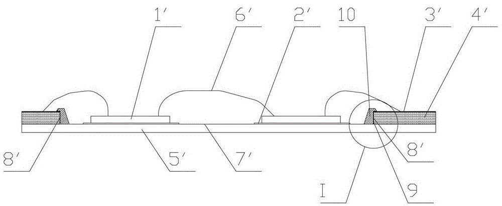
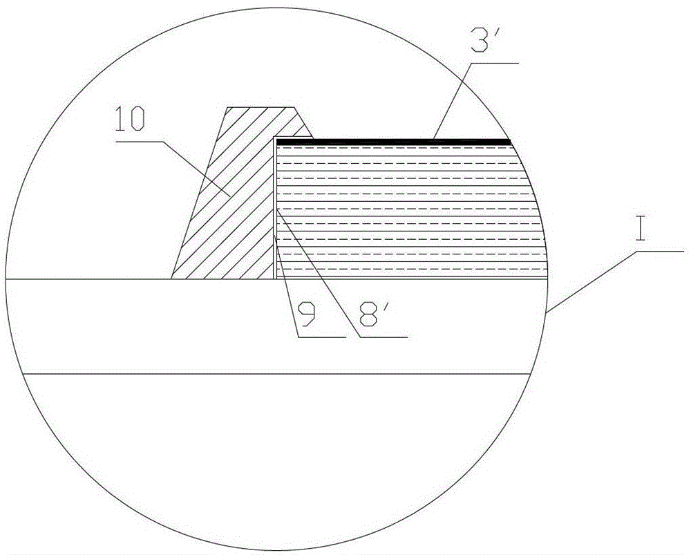
[0027] like figure 2 , image 3 As shown, a COBLED packaging structure includes an aluminum substrate 5', a glass fiber layer 4' and a wafer 1' are arranged on the aluminum substrate 5', and a metal ring 10 is arranged on the glass fiber surface 8' inside the glass fiber layer 4' , the metal ring 10 is bonded to the glass fiber surface 8 ′ through insulating glue 9 , and the wafer 1 ′ is located inside the metal ring 10 . In this COBLED packaging structure, the metal ring 10 is arranged on the glass fiber surface 8', and the metal ring 10 is bonded and fixed to the glass fiber surface 8' through the die-bonding glue 2', so that the chip 1' is located inside the metal ring 10 , not only isolate the glass fiber surface 8' from the chip 1', avoid the glass fiber surface 8' from being exposed, and then prevent the glass fiber layer 8' from being...


PUM

PropertyMeasurementUnit
thicknessaaaaaaaaaa

Abstract

The present invention relates to a COB LED packaging structure, comprising an aluminum substrate, a glass fiber layer and a chip are arranged on the aluminum substrate, and a metal ring is arranged on the glass fiber surface inside the glass fiber layer, and the metal ring is passed through the crystal bonding process. Glue is bonded to the glass fiber surface, and the wafer is located inside the metal ring. The present invention also relates to a COB LED packaging process, a COB LED packaging process for manufacturing the COB LED packaging structure, including the following steps: Step A: Substrate production, after pre-pressing the aluminum substrate and the glass fiber layer , set the metal ring on the glass fiber surface inside the glass fiber layer, and bond the metal ring to the glass fiber surface through insulating glue; Die bond wires so that the die is located inside the metal ring. The process of the COB LED packaging process is simple and easy to implement, and the COB LED packaging structure obtained through the COB LED packaging process has high light extraction efficiency and simple structure.

Description

technical field [0001] The invention relates to the field of LED packaging, in particular to a COB LED packaging structure and packaging technology. Background technique [0002] COBLED (ChipOnBoard, chip-on-board package), the bare chip is adhered to the interconnected substrate with conductive or non-conductive adhesive, and then wire bonded to achieve its electrical connection. COBLED is also called COBLEDsource, or COBLEDmodule. [0003] like figure 1 As shown, the existing COBLED packaging mostly uses an aluminum substrate 5 with high reflectivity as the substrate, on which the chip 1 is bonded with a die-bonding glue 2, and a layer of insulating material is laminated on the aluminum substrate 5. Glass fiber layer 4, copper foil 3 is arranged on the glass fiber layer 4, the chip 1 is positioned at the inner side of the glass fiber surface 8 of the glass fiber layer 4, and the chip 1 is electrically connected with the copper foil 3 through the gold wire 6; A reflective...

Claims


Application Information

Patent Timeline
Patent Type & Authority Patents(China)
IPC IPC(8): H01L33/48H01L33/54H01L33/60
CPCH01L2224/48091H01L2224/48137H01L2924/00014
Inventor 付晓辉付建国
Owner SHENZHEN HUAGAO OPTOELECTRONICS TECH
Why Eureka
Try Eureka