Electronic component

a technology of electronic components and components, applied in the field of electronic components, can solve the problems of reducing the qs of all resonators, and difficulty in achieving desired filter characteristics

Active Publication Date: 2011-09-13
TDK CORPARATION
View PDF9 Cites 0 Cited by
  • Summary
  • Abstract
  • Description
  • Claims
  • Application Information

AI Technical Summary

Benefits of technology

[0014]It is an object of the present invention to provide an electronic component including at least one resonator provided within a layered substrate, the electronic component being capable of increasing the Q of the resonator connected to a terminal used for at least one of input and output of signals.
[0020]According to the first electronic component of the present invention, the terminal used for at least one of input and output of signals is directly connected to all of the resonator-forming conductor layers of the first type. This serves to increase the Q of the resonator connected to the terminal.
[0021]According to the second electronic component of the present invention, the input terminal is directly connected to all of the resonator-forming conductor layers of the first type of the first resonator, and the output terminal is directly connected to all of the resonator-forming conductor layers of the third type of the second resonator. This serves to increase the Qs of the first and second resonators.

Problems solved by technology

If this is done, however, the inductive coupling between every adjacent resonators becomes too strong, so that it becomes difficult to attain desired filter characteristics.
Specifically, the passband width of the filter becomes too broad if the inductive coupling between adjacent resonators becomes too strong.
However, this reduces the Qs of all of the resonators.
This configuration cannot greatly increase the Q of the resonator connected to the terminal for input or output of signals.

Method used


Image

  • Electronic component
  • Electronic component
  • Electronic component

Examples


Embodiment Construction

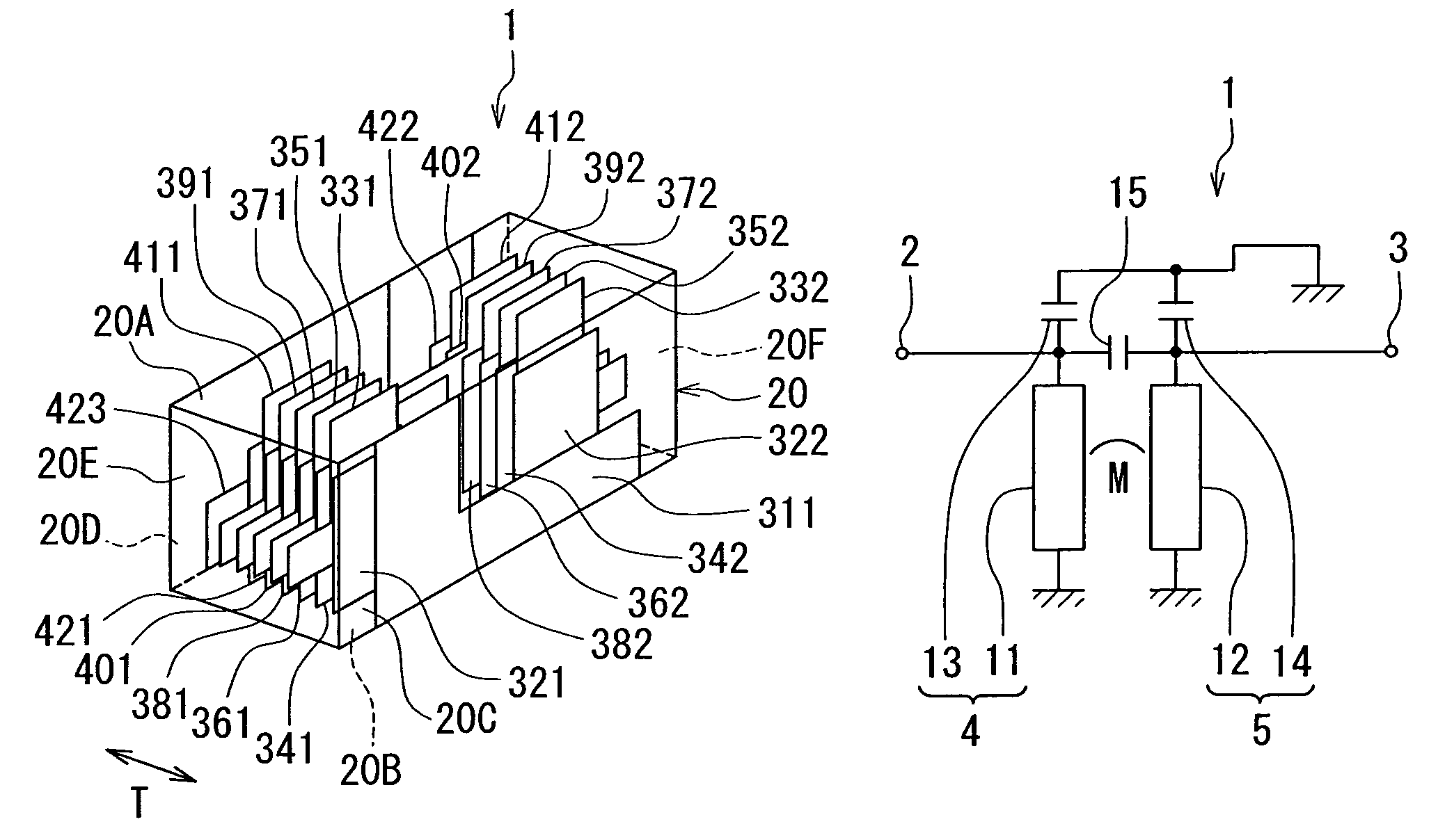
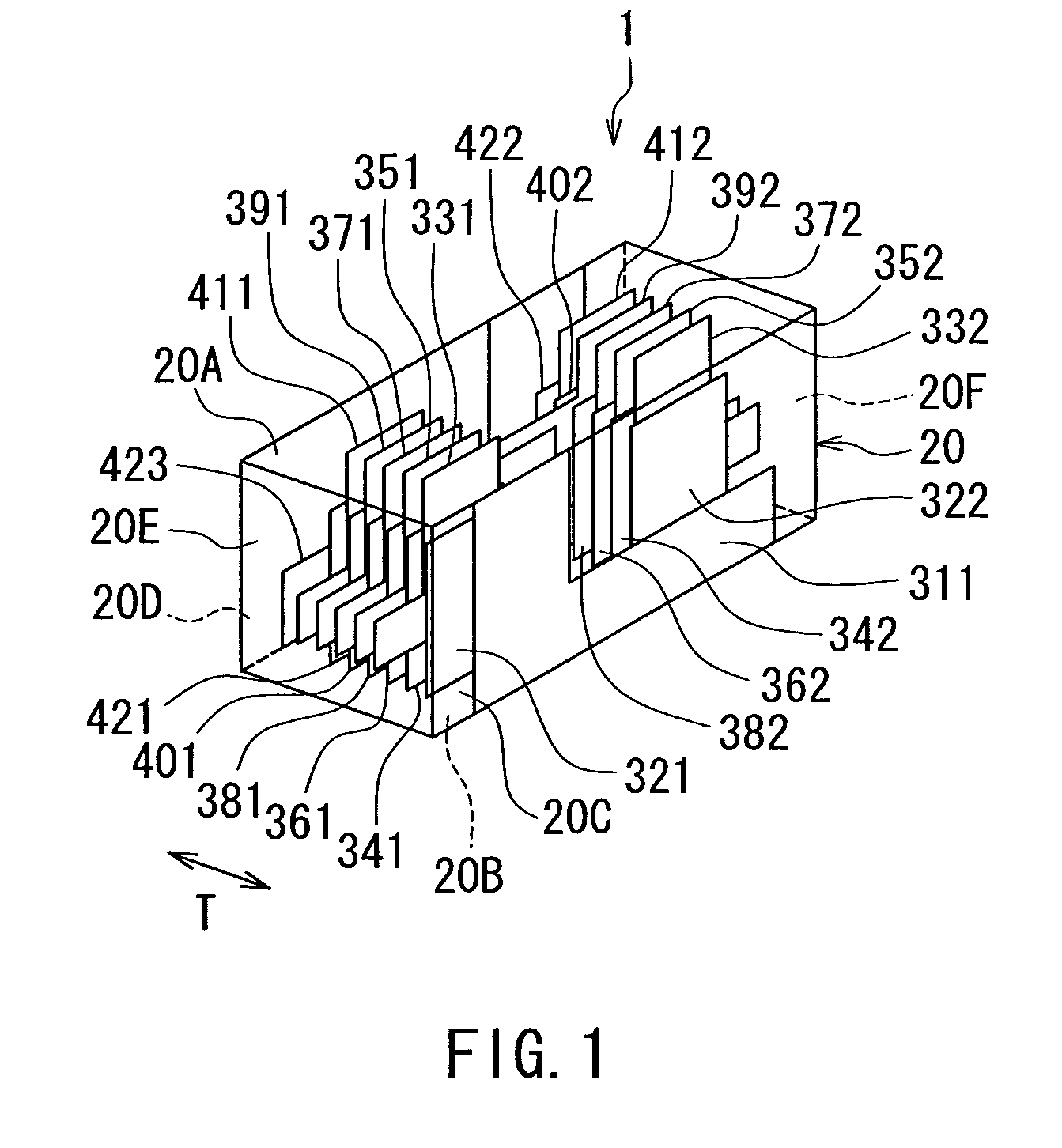
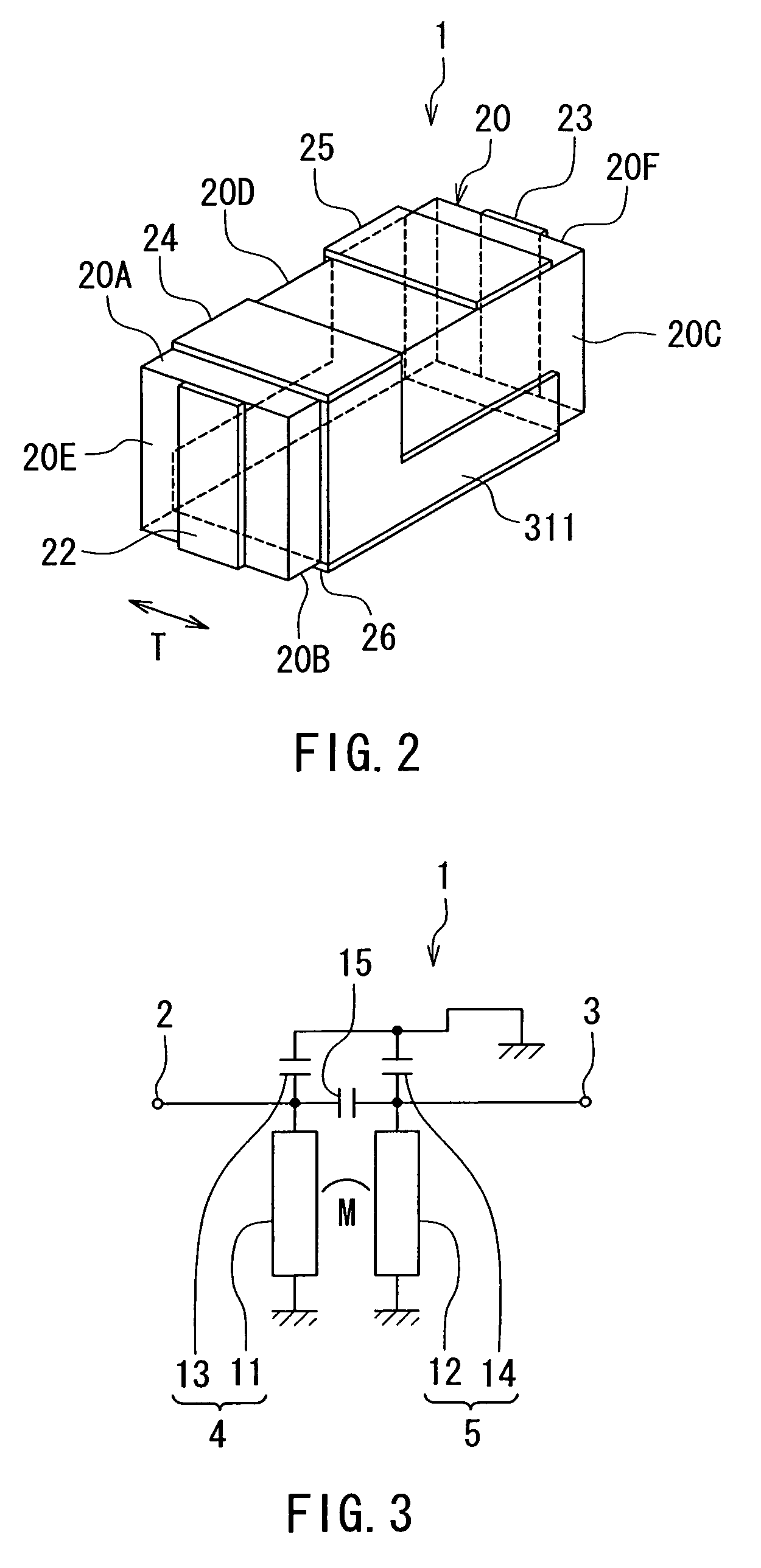
[0039]A preferred embodiment of the present invention will now be described in detail with reference to the drawings. Reference is first made to FIG. 3 to describe the circuit configuration of an electronic component of the preferred embodiment of the invention. The electronic component 1 of the present embodiment has the function of a bandpass filter. As shown in FIG. 3, the electronic component 1 includes an input terminal 2 used for input of signals, an output terminal 3 used for output of signals, two resonators 4 and 5, and a capacitor 15.

[0040]The resonator 4 includes an inductor 11 and a capacitor 13. The resonator 5 includes an inductor 12 and a capacitor 14. The resonators 4 and 5 are inductively coupled to each other. The inductors 11 and 12 are also inductively coupled to each other. In FIG. 3 the inductive coupling between the inductors 11 and 12 is shown with a curve M.

[0041]One end of the inductor 11 and one end of each of the capacitors 13 and 15 are connected to the ...


PUM


Abstract

An electronic component includes first and second resonators provided within a layered substrate including stacked dielectric layers. The first resonator includes resonator-forming conductor layers of a first type and a second type. The resonator-forming conductor layers of the first type and the second type are reversed in relative positions of the short-circuited end and the open-circuited end, and are alternately arranged in the stacking direction of the dielectric layers. An input terminal is connected to all of the resonator-forming conductor layers of the first type. The second resonator includes resonator-forming conductor layers of a third type and a fourth type. The resonator-forming conductor layers of the third type and the fourth type are reversed in relative positions of the short-circuited end and the open-circuited end, and are alternately arranged in the stacking direction of the dielectric layers. An output terminal is connected to all of the resonator-forming conductor layers of the third type.

Description

BACKGROUND OF THE INVENTION[0001]1. Field of the Invention[0002]The present invention relates to an electronic component including a plurality of resonators provided within a layered substrate.[0003]2. Description of the Related Art[0004]There are strong demands for reductions in size and thickness of communication apparatuses for short-range wireless communications, such as communication apparatuses conforming to the Bluetooth standard and communication apparatuses for use on a wireless local area network (LAN). Accordingly, reductions in size and thickness are also demanded of electronic components incorporated in such communication apparatuses. A bandpass filter that filters reception signals is one of electronic components incorporated in the communication apparatuses mentioned above. Reductions in size and thickness are also demanded of the bandpass filter. To meet the demands, a layered filter including a plurality of resonators each formed using at least one conductor layer o...

Claims


Application Information

Patent Timeline
Patent Type & Authority Patents(United States)
IPC IPC(8): H01P1/205H01P7/08
CPCH01P1/20327
Inventor TOMAKI, SHIGEMITSUOOTSUKA, NORIAKITSUYA, YOSHIKAZUSHINODA, KAZUSHIGE
Owner TDK CORPARATION
Why Eureka
Try Eureka