Opto-electronic oscillator and method

an opto-electronic and oscillator technology, applied in the field of opto-electronic oscillator circuits, can solve the problems of increasing the total q, and achieve the effect of increasing the output rf oscillation stability, increasing the immunity of the circuit to noise, and increasing the equivalent round trip delay of the optical signal

Active Publication Date: 2014-09-23
THE BOARD OF TRUSTEES OF THE UNIV OF ILLINOIS
View PDF32 Cites 1 Cited by
  • Summary
  • Abstract
  • Description
  • Claims
  • Application Information

AI Technical Summary

Benefits of technology

[0007]In accordance with a form of the invention, there is provided, a scalable differential triple-loop architecture that has features including the following: (1) The architecture of an embodiment hereof takes advantages of three loops (electronic, opto-electronic and purely optical) that are fundamentally injection locked together to increase the output RF oscillation stability. (2) A differential oscillator of an embodiment hereof increases the circuit's immunity to noise resulting from power supply and ground potential fluctuations, and also increases the equivalent round trip delay of the optical signal in the loop, increasing the total Q. (3) The fundamental architecture of an embodiment hereof is developed as a unit cell that can easily be cascaded. By cascading multiple identical cells, it is possible to achieve an RF phase noise that is reduced proportional to the square of the number of cells in the architecture. The paradigm of cascading multiple unit cells can therefore be used to great advantage in achieving an RF output with ultra low phase noise performance.

Problems solved by technology

(2) A differential oscillator of an embodiment hereof increases the circuit's immunity to noise resulting from power supply and ground potential fluctuations, and also increases the equivalent round trip delay of the optical signal in the loop, increasing the total Q.

Method used


Image

  • Opto-electronic oscillator and method
  • Opto-electronic oscillator and method
  • Opto-electronic oscillator and method

Examples


Embodiment Construction

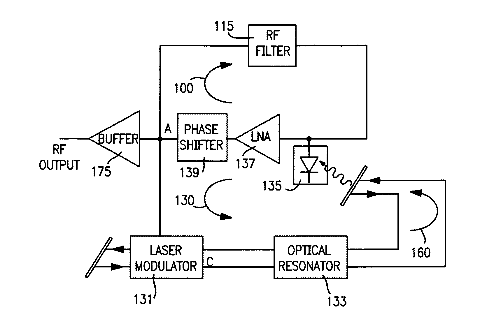
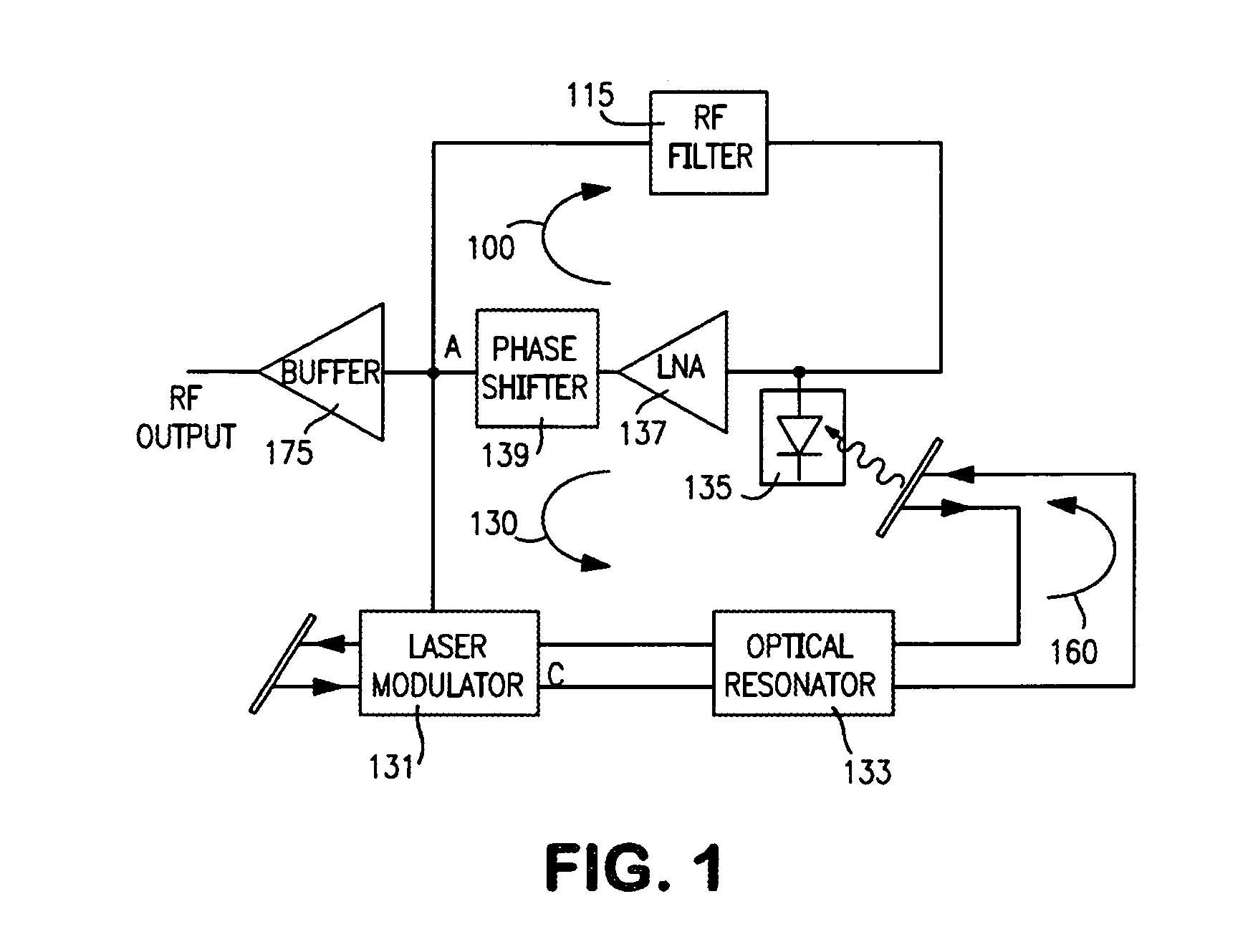
[0022]An embodiment showing the triple loop nature of the half-circuit unit cell is illustrated in FIG. 1. The half-cell architecture of this embodiment includes three loops: an RF loop 100, an opto-electronic loop 130, and an optical loop 160. The opto-electronic loop in the opto-electronic oscillator (OEO) topology includes a laser modulator 131, a high Q optical resonator 133, a photodetector 135, a low noise amplifier (LNA) 137 and a phase shifter 139. Though the LNA provides rudimentary RF filtering, the present embodiment includes the addition of an electrical RF loop (100) coupled with the opto-electronic loop (130). This electronic loop 100 includes RF filter 115 and performs a filtering function to select the RF optical mode. The loop 160 is a purely optical loop, which, as noted above, contains laser modulator 131 (which is preferably a transistor laser modulator), and high-Q optical resonator 133, as well as optical feedback. Note that there is no O / E or E / O conversion in...


PUM

PropertyMeasurementUnit
impedanceaaaaaaaaaa
phaseaaaaaaaaaa
lengthsaaaaaaaaaa

Abstract

An opto-electronic oscillator circuit, including: an opto-electronic circuit loop including an optical modulator that receives a first electrical signal and produces an optical output signal coupled with an optical resonator, a photodetector circuit optically coupled with the optical resonator, and a phase shifter coupled with the photodetector circuit for producing a phase shifted output signal that is fed back as the first electrical signal; an optical loop comprising the optical coupling of the optical resonator with the photodetector; and an electrical feedback circuit loop for coupling the first electrical signal with the photodetector circuit.

Description

PRIORITY CLAIMS[0001]Priority is claimed from U.S. Provisional Patent Application No. 61 / 627,230, filed Oct. 7, 2011 and priority is also claimed from U.S. Provisional Patent Application No. 61 / 686,202, filed Mar. 30, 2012, and both of said U.S. Provisional Patent Applications are incorporated herein by reference.RELATED APPLICATIONS[0002]Some of the subject matter of the present Application is related to some of the subject matter of the U.S. patent application Ser. No. 13 / 633,383, filed of even date herewith, and assigned to the same assignee as the present Application.FIELD OF THE INVENTION[0003]This invention relates to the field of oscillator circuits, systems, and methods and, more particularly, to opto-electronic oscillator circuits, systems and methods that exhibit ultra-low phase noise and ultra-stable frequency output.BACKGROUND OF THE INVENTION[0004]There are numerous applications where very high frequency signals, with ultra-low phase noise and ultra-stability of frequen...

Claims


Application Information

Patent Timeline
Patent Type & Authority Patents(United States)
IPC IPC(8): H01S3/30H01S3/00G02F1/01H03D9/00
CPCG02F1/0123H03D9/00
Inventor FENG, MILTONHOLONYAK, JR., NICKTHEN, HAN WUISTUENKEL, MARKTAN, FEI
Owner THE BOARD OF TRUSTEES OF THE UNIV OF ILLINOIS
Why Eureka
Try Eureka