Image display device and method of controlling the same
a technology of image display and video signal, which is applied in the field of image display devices, can solve the problems of insufficient light emission of luminescent elements and difficulty in storing exact potentials, and achieve the effect of high-quality image display reflecting video signals
- Summary
- Abstract
- Description
- Claims
- Application Information
AI Technical Summary
Benefits of technology
Problems solved by technology
Method used
Image

Examples
embodiment 1
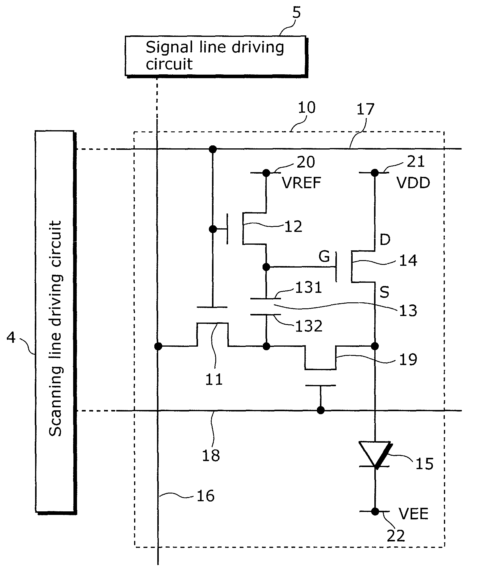
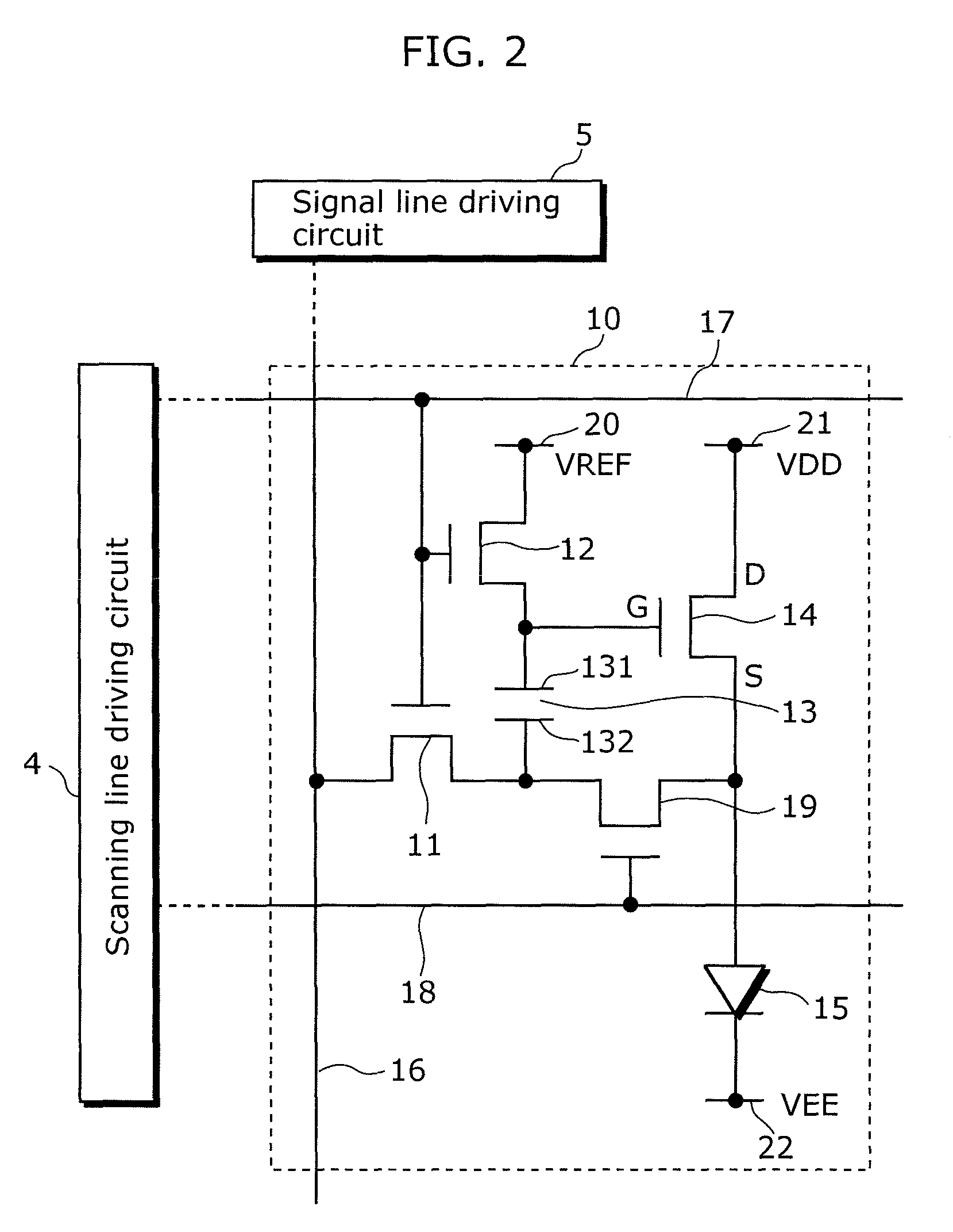
[0075]An image display device in this embodiment includes luminescence pixels arranged in a matrix. Each of the luminescence pixels includes: a luminescence element; a capacitor; a driving element having a gate connected to a first electrode of the capacitor and having a source connected to the luminescence element; a third switching element for switching between conductive and non-conductive states between the source of the driving element and the second electrode of the capacitor; a first switching element for switching between conductive and non-conductive states between a reference power source line and a first electrode of the capacitor; and a second switching element for switching between conductive and non-conductive states between a data line and a second electrode of the capacitor. This configuration enables storage of an accurate potential corresponding to a signal voltage onto both end terminals of the capacitor. This makes it possible to achieve an accurate image display...
embodiment 2
[0117]An image display device in this embodiment includes luminous pixels arranged in a matrix. Each of the luminous pixels includes: a luminescence element; a capacitor; a driving element having a gate connected to a first electrode of the capacitor and having a source connected to the luminescence element; a third switching element for switching between conductive and non-conductive states between the source of the driving element and the second electrode of the capacitor; a first switching element for switching between conductive and non-conductive states between a reference power source line and a second electrode of the capacitor; and a second switching element for switching between conductive and non-conductive states between a data line and a first electrode of the capacitor. This configuration enables storage of an accurate potential corresponding to a signal voltage onto both end terminals of the capacitor. This makes it possible to achieve an accurate image display reflect...
embodiment 3
[0151]An image display device in this embodiment includes luminescence pixels arranged in a matrix. Each of the luminous pixels includes: a luminescence element; a capacitor; a driving element having a gate connected to a first electrode of the capacitor and having a source connected to the luminescence element; a third switching element for switching between conductive and non-conductive states between the source of the driving element and the second electrode of the capacitor; a first switching element for switching between conductive and non-conductive states between a first reference power source line and a first electrode of the capacitor; a second switching element for switching between conductive and non-conductive states between a data line and a second electrode of the capacitor, and a second capacitor connected to between the second electrode of the capacitor and the second reference power source line. This configuration enables storage of an accurate potential correspondi...
PUM
 Abstract
Description
Claims
Application Information
 - R&D
- Intellectual Property
- Life Sciences
- Materials
- Tech Scout
- Unparalleled Data Quality
- Higher Quality Content
- 60% Fewer Hallucinations
Browse by: Latest US Patents, China's latest patents, Technical Efficacy Thesaurus, Application Domain, Technology Topic, Popular Technical Reports.
© 2025 PatSnap. All rights reserved.Legal|Privacy policy|Modern Slavery Act Transparency Statement|Sitemap|About US| Contact US: help@patsnap.com