Solid-state imaging device, drive method therefor, and electronic device

a solid-state imaging and drive method technology, applied in semiconductor devices, diodes, color signal processing circuits, etc., can solve the problems of inability to detect the leakage light for each pixel, and the inability to correct the degraded image quality from the leakage ligh

Active Publication Date: 2011-01-27
SONY SEMICON SOLUTIONS CORP
View PDF14 Cites 43 Cited by
  • Summary
  • Abstract
  • Description
  • Claims
  • Application Information

AI Technical Summary

Problems solved by technology

In the CCD solid-state imaging device having a vertical transfer register to ensure global shutter imaging, light leaks into the vertical transfer register, causing a smear.
Since a signal (smear) originated from light leaked into each pixel is not transferred to an optical black pixel region in the CMOS solid-state imaging device, leak light for each pixel cannot be detected.
As a result, the CMOS solid-state imaging device capable of implement global shutter imaging has a problem that the degraded image quality originated from the leak light cannot be corrected.

Method used


Image

  • Solid-state imaging device, drive method therefor, and electronic device
  • Solid-state imaging device, drive method therefor, and electronic device
  • Solid-state imaging device, drive method therefor, and electronic device

Examples


third embodiment (

[0035] 5. Third Embodiment (Configurational Example of Solid-state Imaging Device)

fourth embodiment (

[0036] 6. Fourth Embodiment (Configurational Example of Electronic Device)<

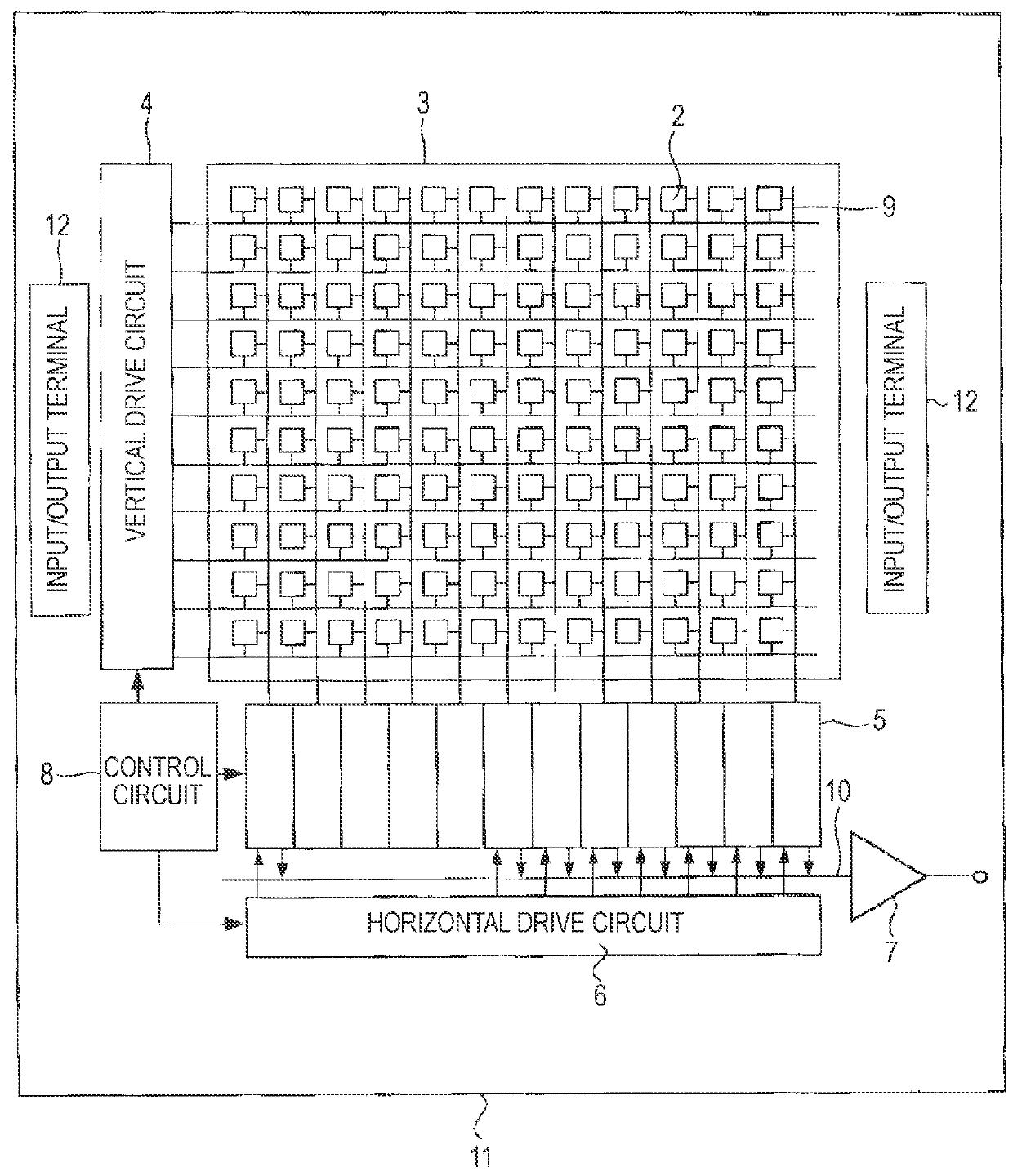
1. Schematic Configurational Example of CMOS Solid-State Imaging Device

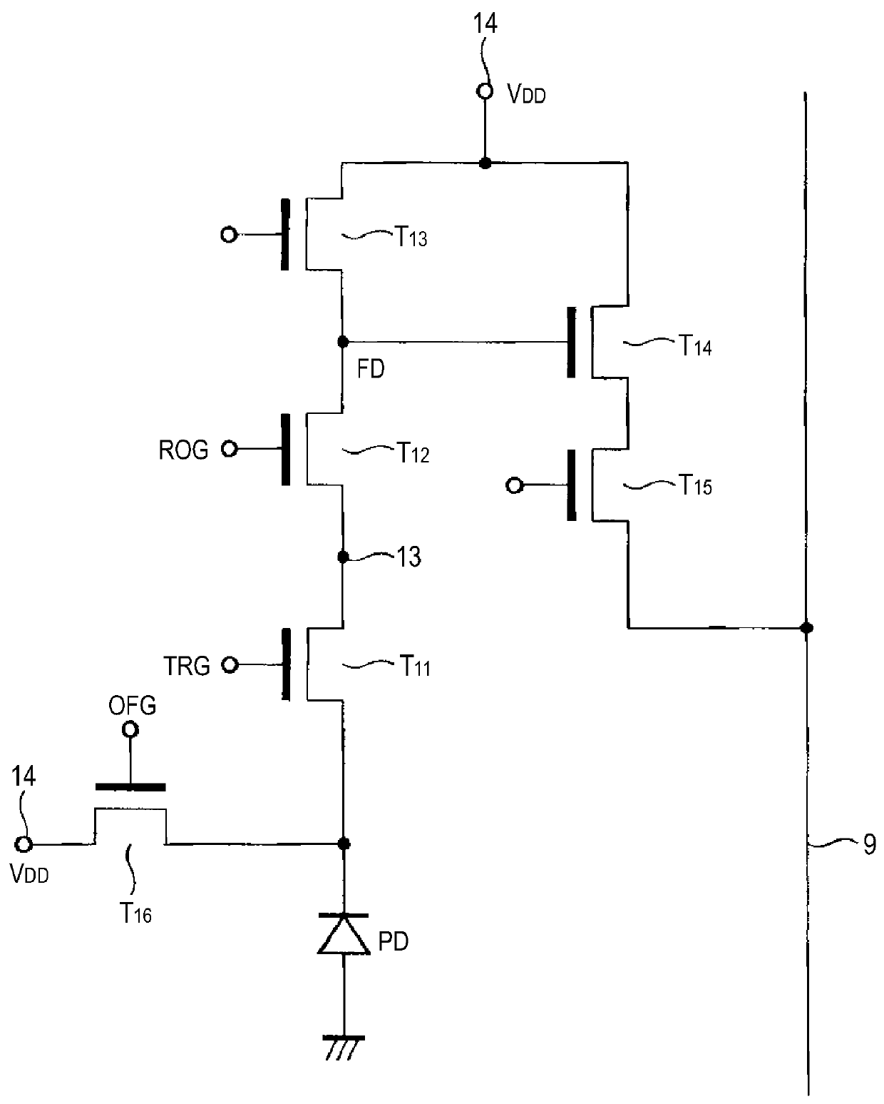
[0037] FIG. 1 shows the schematic configuration of one example of a CMOS solid-state imaging device which is applied to individual embodiments of the invention. As shown in FIG. 1, a solid-state imaging device 1 according to the embodiment is configured to include a pixel section (so-called imaging region) 3 having a plurality of pixels 2, each including a photoelectric conversion part, arranged regularly in a two-dimensional array on a semiconductor substrate 11, for example, a silicon substrate, and a peripheral circuit part. An example of the circuit configuration of the pixel 2 will be described later.

[0038] The peripheral circuit part is configured to include a vertical drive circuit 4, a column signal processing circuit 5, a horizontal drive circuit 6, an output circuit 7, and a control circuit 8.

[0039] The control circuit 8 receives...

first embodiment

3. First Embodiment

[Configurational Example of Solid-State Imaging Device]

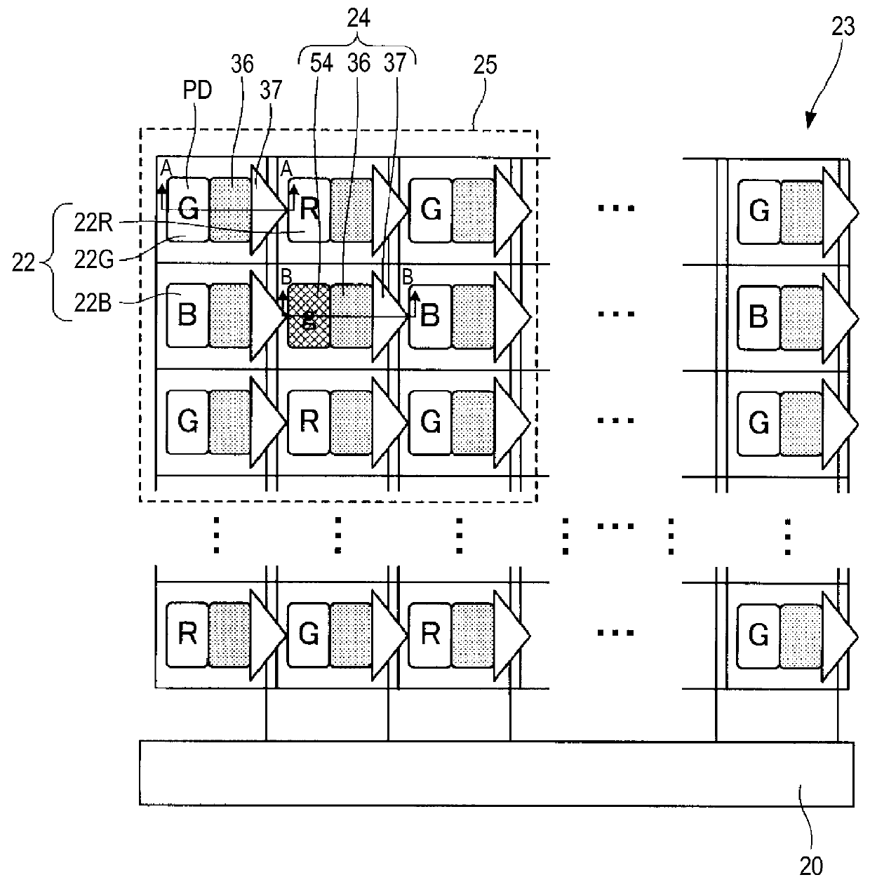
[0055] FIGS. 4 and 5 show a solid-state imaging device according to the first embodiment of the invention. The first embodiment employs a configuration having the pixel layout pattern shown in FIG. 3. FIG. 4 shows the cross section of the essential portion of a normal pixel corresponding to the line A-A in FIG. 3, and FIG. 5 shows the cross section of the essential portion of a leak-light correcting pixel corresponding to the line B-B in FIG. 3.

[0056] A solid-state imaging device 31 according to the first embodiment has a semiconductor substrate 32 of a first conductivity type, e.g., an n-type, in which a semiconductor well region 33 of a second conductivity type, e.g., a p-type, is formed, and has a normal pixel 22 and a leak-light correcting pixel 24 arranged in the p-type semiconductor well region 33 in the pixel layout pattern shown in FIG. 3.

[0057] As shown in FIG. 4, the normal pixel 22 [22R, 22G, 22B] h...


PUM


Abstract

A solid-state imaging device includes: a normal pixel disposed in a pixel section capable of performing a global shutter, and including at least a photoelectric conversion part and a memory part adjacent to the photoelectric conversion part; and a leak-light correcting pixel disposed in the pixel section to correct degradation of an image quality originated from leak light leaked into the memory part.

Description

[0001] 1. Field of the Invention[0002] The present invention relates to a solid-state imaging device, a drive method therefor, and an electronic device equipped with the solid-state imaging device.[0003] 2. Description of the Related Art[0004] Solid-state imaging devices are roughly classified into two types of solid-state imaging devices typified by a CCD (Charge Coupled Device) image sensor and a CMOS (Complementary Metal Oxide Semiconductor) image sensor. Those solid-state imaging devices are widely used in digital still cameras, digital video cameras, and so forth. Recently, from the viewpoints of a lower supply voltage and lower power consumption, MOS type image sensors are used more as solid-state imaging devices to be installed in mobile devices, such as camera-equipped cellular phones.[0005] As a CMOS solid-state imaging device which achieves simultaneous storage in the individual pixels, a CMOS solid-state imaging device has been proposed which has a memory element (capacit...

Claims


Application Information

Patent Timeline
Patent Type & Authority Applications(United States)
IPC IPC(8): H04N9/64
CPCH01L27/14609H01L27/14621H01L27/14656H01L27/14643H01L27/14623
Inventor OKUNO, JUN
Owner SONY SEMICON SOLUTIONS CORP
Why Eureka
Try Eureka