Integrated circuit structure and manufacturing method thereof

a technology of integrated circuits and manufacturing methods, applied in the direction of electrical equipment, semiconductor devices, semiconductor/solid-state device details, etc., can solve the problems of poor adhesion of low-k dielectric layers and silicon oxide dielectric layers, increase in interconnections, and jump in resistance/capacitance (rc) of devices, so as to minimize the peeling of the dielectric layer and enhance the adhesion

Active Publication Date: 2011-10-04
MARLIN SEMICON LTD
View PDF15 Cites 0 Cited by
  • Summary
  • Abstract
  • Description
  • Claims
  • Application Information

AI Technical Summary

Benefits of technology

[0007]Accordingly, the present invention is directed to an integrated circuit structure that uses a protruding bonding portion at the bottom of a plug to connect with a conductive structure so as to enhance adhesion between a dielectric layer and a low dielectric constant dielectric layer and minimize peeling of the dielectric layer.
[0027]In the present invention, a protruding bonding portion is formed on the bottom of the plug. Therefore, the plug can create a tight connection with the conductive structure below and reinforce the adhesion between the dielectric layer and the low-k dielectric layer. As a result, the probability of dielectric peeling is reduced and the performance and product yield of the device is increased.

Problems solved by technology

Because of the miniaturization and the increase in the integration of devices, the density of interconnects also increases and leads to a jump in the resistance / capacitance (RC) of the devices.
However, the adhesion of a low-k dielectric layer and a silicon oxide dielectric layer is poor and the serious effect caused by dielectric peeling leads to the drop of particles and the bridging between metals from the subsequently copper interconnect process.
Therefore, the probability of resulting in a short circuit between some of the copper wires is increased and the process yield can be adversely affected.

Method used


Image

  • Integrated circuit structure and manufacturing method thereof
  • Integrated circuit structure and manufacturing method thereof
  • Integrated circuit structure and manufacturing method thereof

Examples


Embodiment Construction

[0033]Reference will now be made in detail to the present preferred embodiments of the invention, examples of which are illustrated in the accompanying drawings. Wherever possible, the same reference numbers are used in the drawings and the description to refer to the same or like parts.

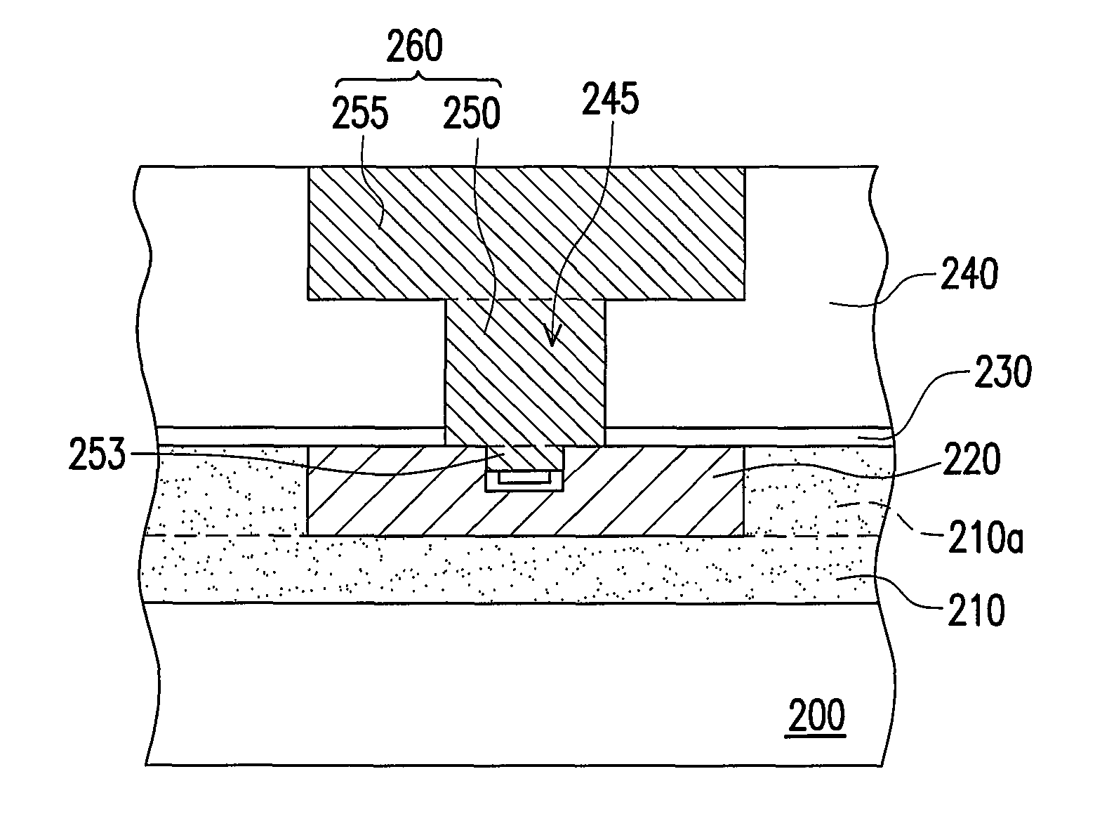
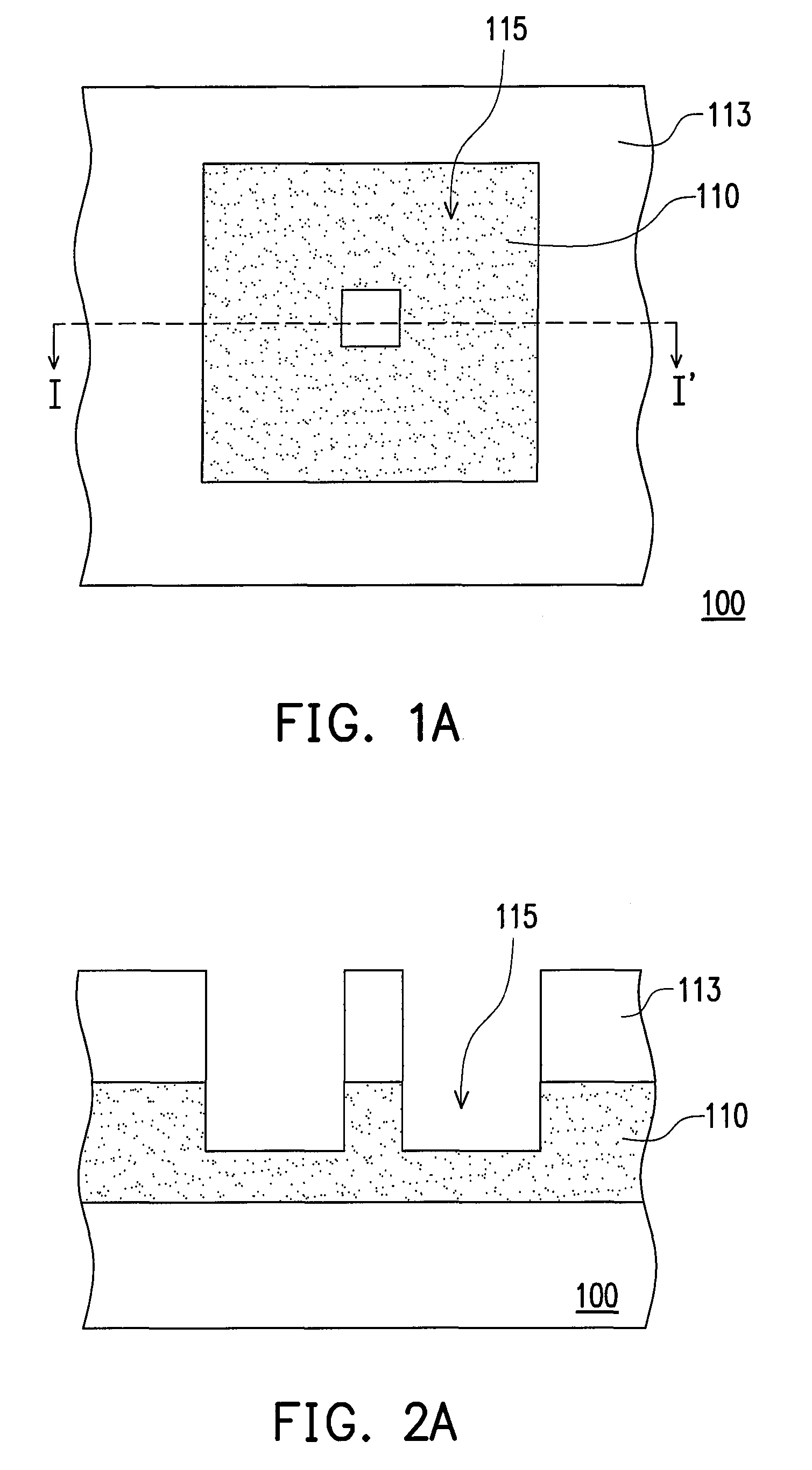
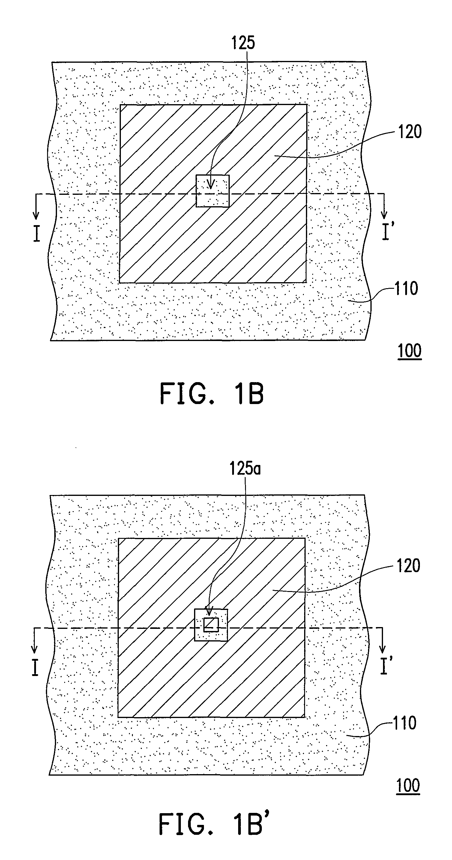
[0034]FIGS. 1A to 1E are top views showing a process of manufacturing an integrated circuit structure according to an embodiment of the present invention. FIGS. 2A to 2E are schematic cross-sectional views along line I-I′ of FIGS. 1A to 1E showing the process of manufacturing an integrated circuit structure.

[0035]As shown in FIGS. 1A and 2A, the present invention provides a method of manufacturing an integrated circuit structure. The method includes providing a dielectric layer 110. The dielectric layer 110 is fabricated using a dielectric material such as silicon oxide, borophosphosilicate glass (BPSG), phosphosilicate glass (PSG) or borosilicate glass (BSG) and formed by performing a chemical vapor...


PUM


Abstract

An integrated circuit structure is provided. The integrated circuit structure includes a dielectric layer, a conductive structure, a low-k dielectric layer and a plug. The conductive structure is disposed in the dielectric layer, having a recess portion. The low-k dielectric layer is disposed on the dielectric layer. The plug is disposed in the low-k dielectric layer and has a protruding bonding portion on the bottom of the plug. The bonding portion is extended into the dielectric layer and connected to the recess portion of the conductive structure.

Description

BACKGROUND OF THE INVENTION[0001]1. Field of the Invention[0002]The present invention generally relates to an integrated circuit structure and a manufacturing method thereof, more particularly, to an interconnect-related integrated circuit structure and manufacturing method thereof.[0003]2. Description of Related Art[0004]In deep sub-micro integrated circuit technology, high-speed, multi-function, highly integrated, low power consumption and low cost ultra large scale integrated circuit chips are mass-produced as a result of the continuous reduction of device line width. Because of the miniaturization and the increase in the integration of devices, the density of interconnects also increases and leads to a jump in the resistance / capacitance (RC) of the devices. As a result, signal transmission or RC delay is increasingly important and the operating efficiency of the devices is lowered correspondingly.[0005]To limit the effect caused by RC delay, low-k inter-layer dielectric layers a...

Claims


Application Information

Patent Timeline
Patent Type & Authority Patents(United States)
IPC IPC(8): H01L23/52H01L21/4763
CPCH01L21/76805H01L21/76816H01L23/5226H01L23/5329H01L23/53295H01L2924/0002H01L2924/00
Inventor WU, PING-CHANG
Owner MARLIN SEMICON LTD
Why Eureka
Try Eureka