Semiconductor package and method for processing and bonding a wire

a technology of semiconductor packages and wires, which is applied in the direction of semiconductor devices, semiconductor/solid-state device details, electrical apparatus, etc., can solve the problems of limited use of copper bonding wires and damage to the structure of aluminum pads, and achieve the effect of large bonding area and sufficient bonding for

Active Publication Date: 2011-11-08
ADVANCED SEMICON ENG INC
View PDF32 Cites 31 Cited by
  • Summary
  • Abstract
  • Description
  • Claims
  • Application Information

AI Technical Summary

Benefits of technology

[0010]According to the method for bonding a copper bonding wire of the present invention, the force resulted from the copper bonding wire can affect an external tool or mold during the pressing process, clipping process, molding process or patterning process. Thus, the force resulted from the copper bonding wire will not damage the structure of the pad. Furthermore, according to the wire bonding structure of the present invention, there is a bigger bonding area between the pad and the copper bonding wire, i.e. there is a bigger bonding force, thereby keeping sufficient the bonding force between the pad and the copper bonding wire.

Problems solved by technology

However, the copper has disadvantage of insufficient ductility and easy oxidation such that the utilization of the copper bonding wire is restricted.
However, the hardness of the copper is higher than that of the aluminum, and thus the force resulted from the copper bonding wire 20 possibly damages the structure of the aluminum pad 32 during the pressing process.

Method used


Image

  • Semiconductor package and method for processing and bonding a wire
  • Semiconductor package and method for processing and bonding a wire
  • Semiconductor package and method for processing and bonding a wire

Examples


first embodiment

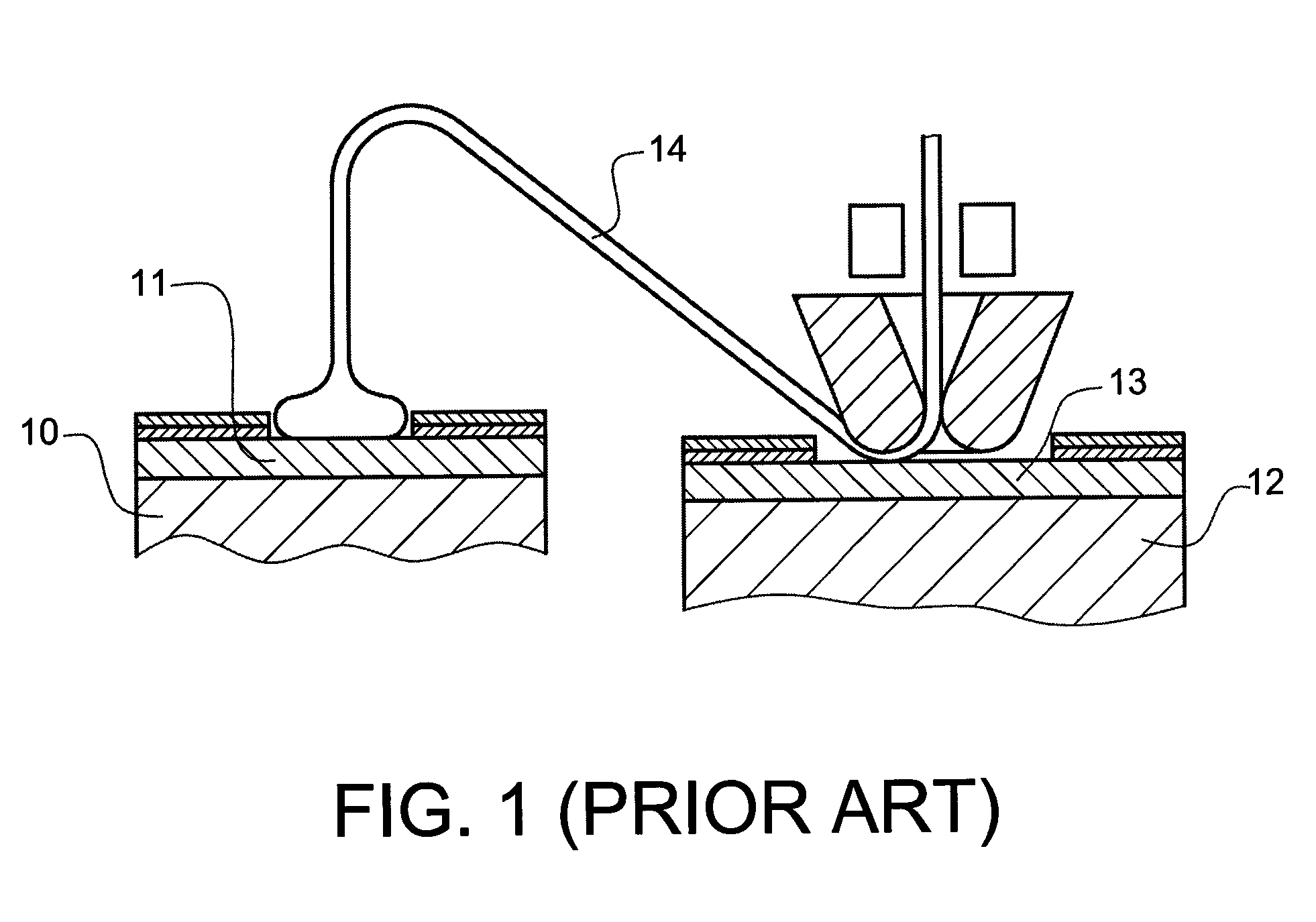
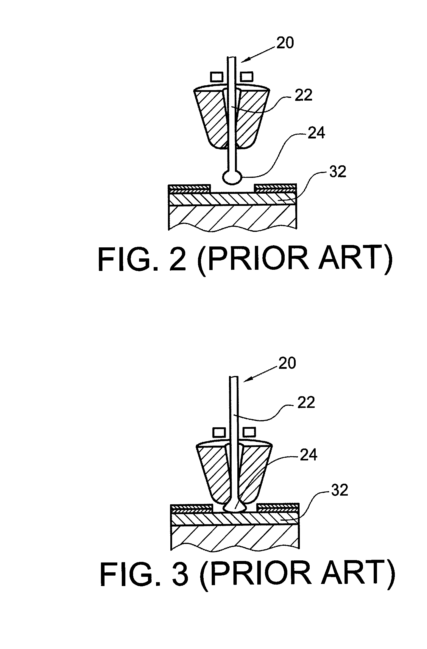
[0027]Referring to FIGS. 14-15, they depict a method for packaging a semiconductor package according to the present invention. Referring to FIG. 14, a carrier 136 is provided, wherein the carrier 136 has an upper surface 113 and a lower surface 114 opposite to the upper surface 113. A chip 110 is disposed on the carrier 136, wherein the chip 110 has an active surface 115 and a back surface 116 opposite to the active surface 115, and the back surface 116 of the chip 110 is located on the upper surface 113 of the carrier 136. The chin 110 includes a pad 262 disposed on the active surface 115. Referring to FIGS. 7a and 7b again, a copper bonding wire 220 of the present invention is formed by pressing, clipping or molding process. The copper bonding wire 220 includes a non-spherical block portion 224′, 224″. Referring to FIG. 15 again, in this embodiment the non-spherical block portion 224″ can be bonded to the pad 232 by a vibration process, so as to finish a method for bonding a bondi...

second embodiment

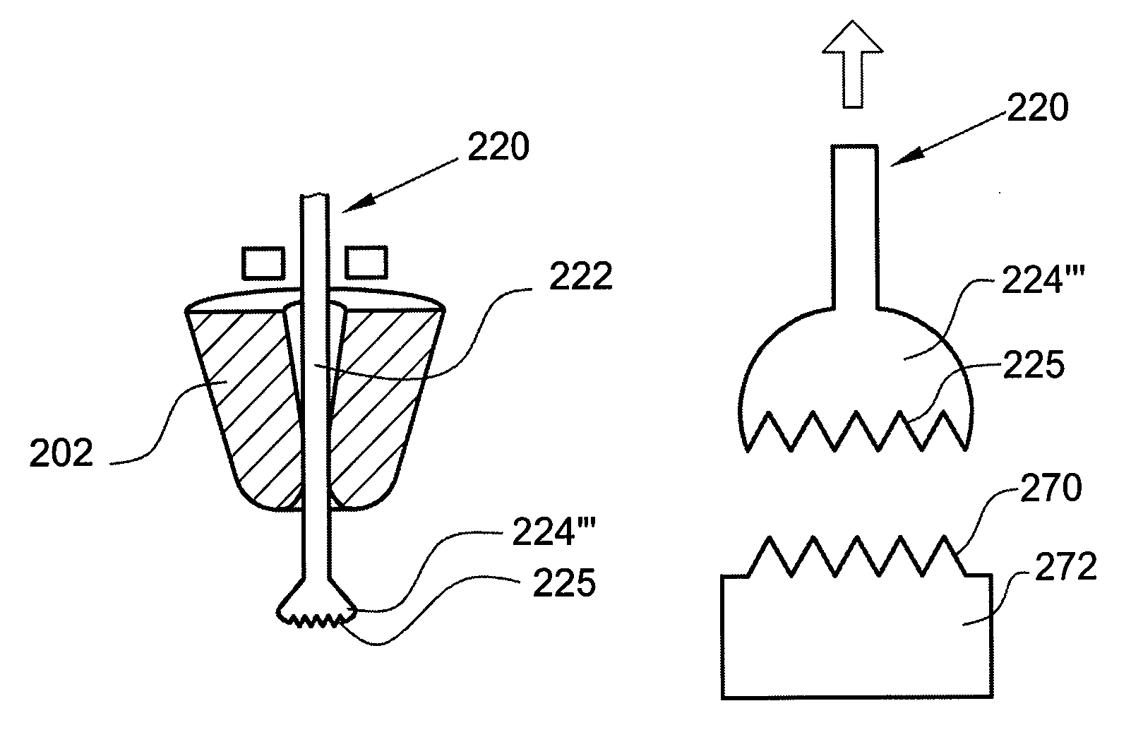
[0031]Referring to FIG. 18, it depicts a method for bonding a copper bonding wire according to a method for packaging a semiconductor package in the present invention. First, a copper bonding wire 220 of the present invention is formed by a patterning process. The copper bonding wire 220 includes a non-spherical block portion 224′″, shown in FIG. 7c. Referring to FIG. 18 again, in this embodiment the non-spherical block portion 224′″ is bonded to a pad 232 by a vibration process, so as to form a wire bonding structure of the present invention.

[0032]If the hardness of the non-spherical block portion 224′″ of the copper bonding wire 220 is more than that of the pad 232 (e.g. aluminum pad), at least one second pattern 233 is formed on a top surface of the pad 232 by the first pattern 225 on the bottom surface of the non-spherical block portion 224′″, and the second pattern 233 is bonded to the first pattern 225. The first and second pattern 225, 233 can has sawtooth-shaped cross-sectio...


PUM


Abstract

A copper bonding wire includes a line portion and a non-spherical block portion. The non-spherical block portion is physically connected to the line portion, and the cross-sectional area of the non-spherical block portion is bigger than that of the line portion.

Description

CROSS REFERENCE TO RELATED APPLICATION[0001]This application claims the priority benefit of U.S. patent application Ser. No. 61 / 079,811, filed on Jul. 11, 2008 and Taiwan Patent Application Serial Number 097133402, filed on Sep. 1, 2008, the full disclosure of which is incorporated herein by reference.BACKGROUND OF THE INVENTION[0002]1. Field of the Invention[0003]The present invention generally relates to a copper bonding wire of a semiconductor package, and more particularly to a wire bonding structure of a semiconductor package, wherein a copper bonding wire includes a non-spherical block portion, whereby the bonding area between a pad and the copper bonding wire can be sufficiently maintained or increased.[0004]2. Description of the Related Art[0005]Referring to FIG. 1, according to a process for manufacturing a semiconductor package, the technology of wire bonding process widely applied to the electrical connection between a pad 11 of a chip 10 and a pad 13 of a substrate 12 by...

Claims


Application Information

Patent Timeline
Patent Type & Authority Patents(United States)
IPC IPC(8): H01L23/48
CPCH01L24/78H01L24/85H01L23/3128H01L24/45H01L2224/05624H01L2224/45147H01L2224/48091H01L2224/48465H01L2224/73265H01L2224/78301H01L2224/85043H01L2224/85045H01L2224/85047H01L2224/85201H01L2224/85365H01L2224/85947H01L2924/01013H01L2924/01029H01L2924/01079H01L2924/15311H01L2924/00014H01L2224/32225H01L2224/48227H01L2924/01019H01L2924/00H01L2224/45144H01L2224/48824H01L2224/48624H01L2924/00012H01L24/48H01L24/73H01L2224/45015H01L2924/181
Inventor CHANG, HSIAO CHUANTSAI, TSUNG YUEHLAI, YI SHAOTONG, HO MINGCHEN, JIAN CHENGYIH, WEI CHIHUNG, CHANG YINGHSU, CHENG TSUNGHUNG, CHIH CHENG
Owner ADVANCED SEMICON ENG INC
Why Eureka
Try Eureka