Semiconductor chip with solder bump and method of fabricating the same

a semiconductor chip and solder bump technology, applied in the field of semiconductor chip with solder bump, can solve the problems of cracks at the bonding interface of the solder bump b>40/b> or inside the solder bump, and achieve the effect of increasing the bonding area and improving the reliability of the semiconductor chip

Inactive Publication Date: 2009-02-05
NEPES CO LTD
View PDF3 Cites 23 Cited by
  • Summary
  • Abstract
  • Description
  • Claims
  • Application Information

AI Technical Summary

Benefits of technology

[0010]Therefore, the present invention has been made in view of the above-mentioned problems, and it is an objective of the present invention to provide a semiconductor chip having a solder bump, in which an adhesion enhance layer (AEL) is formed between an under bump metal (UBM) layer and the solder bump, thereby increasing a bonding area between the solder bump and the UBM layer and the resulting adhesive force. Further, the present invention is directed to form the AEL using a material capable of preventing tin (Sn) in the solder bump from being diffused, thereby improving reliability of the semiconductor chip.Technical Solution
[0012]Thereby, the solder bump is more firmly bonded through the AEL, and thus the reliability of the semiconductor package can be improved.
[0014]Thereby, a bonding area increases through the AEL having the concavo-convex portion, and thus the solder bump is more firmly bonded, so that the reliability of the semiconductor package can be improved.

Problems solved by technology

Hence, the semiconductor package has a size greater than that of the semiconductor chip, and is limited to downsizing and mass-production because it takes much time to complete a wire bonding process.
As a result, a defect in which cracks take place at a bonding interface of the solder bump 40 or inside the solder bump may be caused.

Method used


Image

  • Semiconductor chip with solder bump and method of fabricating the same
  • Semiconductor chip with solder bump and method of fabricating the same
  • Semiconductor chip with solder bump and method of fabricating the same

Examples


Embodiment Construction

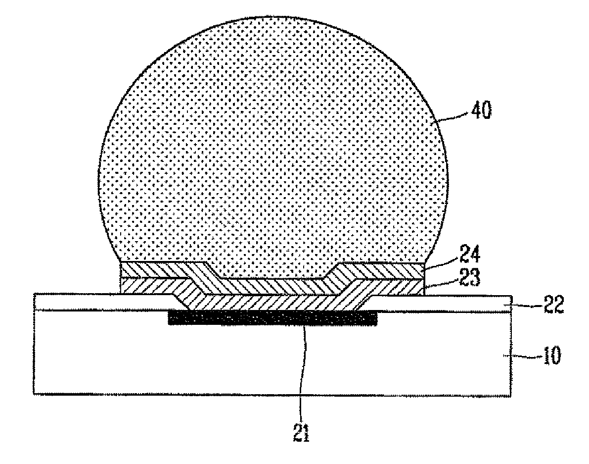
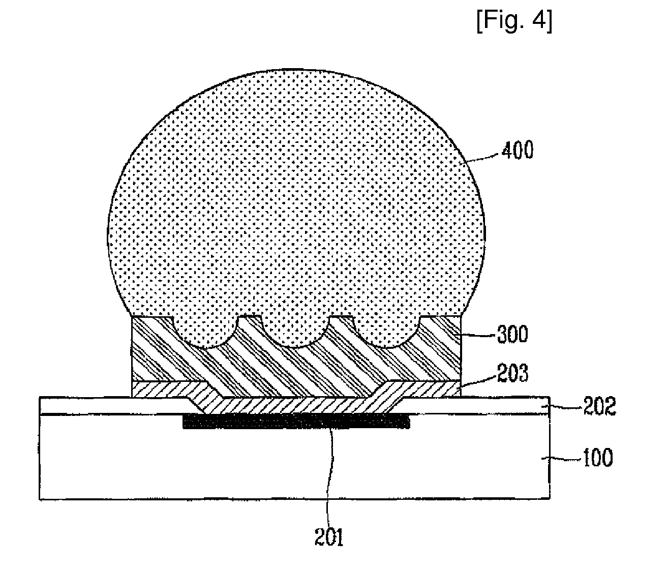
[0031]Reference will now be made in detail to the exemplary embodiments of the present invention.

[0032]FIG. 4 is a sectional view illustrating a semiconductor chip having a solder bump formed on an adhesion enhance layer in accordance with the present invention.

[0033]As shown in FIG. 4, the present invention is characterized in that a solder bump 400 is formed on an adhesion enhance layer (AEL) 300 for reinforcing adhesive force.

[0034]Specifically, the semiconductor chip 100 according to the present invention has at least one electrode pad 201 formed thereon, and the semiconductor chip 100 has a passivation layer 202 formed thereon to allow a top surface of the electrode pad 201 to be exposed. At least one under bump metal (UBM) layer 203 is formed on the electrode pad 201, the top surface of which is exposed by the passivation layer 202. The AEL 300 is formed on the UBM layer 203. The solder bump 400 is formed on the AEL 300.

[0035]Here, the electrode pad 201 may be composed of meta...


PUM


Abstract

A semiconductor chip having a solder bump and a method of fabricating the same are provided. The semiconductor chip includes at least one under bump metal (UBM) layer formed on an electrode pad of the semiconductor chip, an adhesion enhance layer (AEL) formed on the UBM layer and having at least one concavo-convex portion on a top surface thereof, and the solder bump formed on the AEL. Thereby, adhesive solder bump is increased, and thereby the reliability of the semiconductor chip can be improved. Further, it is possible to prevent tin (Sn) in the solder bump from being diffused due to the AEL.

Description

TECHNICAL FIELD[0001]The present invention relates to a semiconductor chip with a solder bump and a method of fabricating the same, and more particularly to a semiconductor chip having a solder bump reinforcing adhesive force and a method of fabricating the same.BACKGROUND ART[0002]In general, a semiconductor package fabricated by a wire bonding technique has electrode terminals of a printed circuit board which are electrically connected with pads of a semiconductor chip by means of conductive wires. Hence, the semiconductor package has a size greater than that of the semiconductor chip, and is limited to downsizing and mass-production because it takes much time to complete a wire bonding process.[0003]Particularly, due to high integration, high performance, and high speed of the semi-conductor chip, various efforts to downsize and mass-produce the semiconductor package are tried. This recent trial results in a proposal for the semiconductor package in which the electrode terminals ...

Claims


Application Information

Patent Timeline
Patent Type & Authority Applications(United States)
IPC IPC(8): H01L21/60H01L23/498
CPCH01L24/11H01L2924/014H01L2224/1308H01L2224/13082H01L2224/13111H01L2224/13116H01L2224/13147H01L2224/13155H01L2224/13164H01L2224/16H01L2924/01013H01L2924/01022H01L2924/01027H01L2924/01029H01L2924/0103H01L2924/01046H01L2924/01047H01L2924/01078H01L2924/01079H01L2924/01082H01L2924/01322H01L2924/10329H01L2224/1147H01L2924/01033H01L2924/01024H01L2924/00013H01L24/13H01L2924/00014H01L2924/01083H01L2224/13099H01L24/03H01L24/05H01L2224/0347H01L2224/03622H01L2224/05001H01L2224/05022H01L2224/051H01L2224/05124H01L2224/05144H01L2224/05147H01L2224/05155H01L2224/05166H01L2224/05171H01L2224/05557H01L2224/05572H01L2224/056H01L2224/05624H01L2224/05647H01L2224/05666F24D3/08F24D3/18F25B30/02
Inventor CHOI, JOON YOUNG
Owner NEPES CO LTD
Why Eureka
Try Eureka